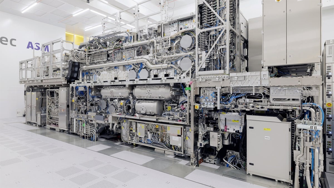
ASML on Wednesday said that it had begun to ship its second High-NA EUV lithography system to another customer. The announcement highlights that there is a major interest for next-generation extreme ultraviolet (EUV) lithography among leading chipmakers. Meanwhile, it is not clear which of ASML's customers is the second company to get an EUV tool with a 0.55 numerical aperture projection optics.
"Regarding High-NA, or 0.55 NA EUV, we shipped our first system to a customer and this system is currently under installation," said Christophe Fouquet, chief business officer of ASML, at the company's earnings conference call with analysts and investors. "We started to ship the second system this month and its installation is also about to start."
ASML began to ship its first High-NA EUV litho tool — the Twinscan EXE:5000 — to Intel at the end of 2023. Intel will use the system to learn how to use such machines and will insert the system into mass production with its Intel 14A fabrication process, which is a few years away. By starting to work on its High-NA EUV-based process technologies early enough, Intel will be able to develop industry-standards for next-generation lithography, which is poised to become a competitive advantage in the coming years.
"During the SPIE industry conference in February, we announced first light on our High-NA system located in our joint ASML-Imec High-NA lab in Veldhoven," said the CBO. "We have since achieved first images, with a new record resolution below 10nm and expect to start exposing wafers in the coming weeks. All High-NA customers will use this system for early access to process development."
While TSMC and Rapidus do not seem to be in hurry to adopt High-NA EUV lithography systems for mass production, they ill still have to do it sometime down the road, which is why ASML is optimistic about the future of this technology. In fact, the world's largest maker of wafer fab tools is exploring Hyper-NA, EUV lithography tools with projection optics featuring numerical aperture with higher than 0.7.
"The customer interest for our [High-NA] system lab is high as this system will help both our Logic and Memory customers prepare for High-NA insertion into their roadmaps," said Fouquet. "Relative to 0.33 NA, the 0.55 NA system provides finer resolution enabling an almost 3x increase in transistor density, at a similar productivity, in support of sub-2nm Logic and sub-10nm DRAM nodes."