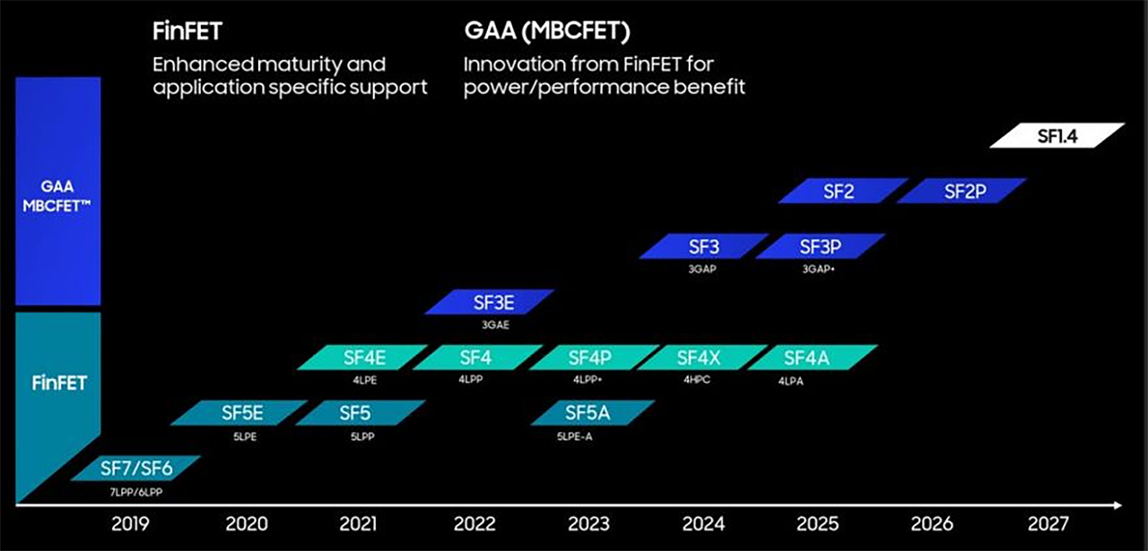
Samsung Foundry has begun trial production of chips on its 2nd Generation 3nm-class process technology known as SF3, reports Chosun, citing unnamed industry sources. The company reportedly aims to achieve a yield of over 60% within the next six months. The information should be taken with a pinch of salt since it comes from an unofficial source. Meanwhile, the SF3 production start is a big deal for Samsung and the industry.
Samsung is reportedly testing the performance and reliability of chips made on its SF3 node. Meanwhile, the first product that Samsung reportedly plans to use its SF3 for is its application processor for wearables, which will be used for the company's upcoming Galaxy Watch 7. Also, the company is expected to use the production node for its Exynos 2500 system-on-chip for Galaxy S25-series smartphones due next year.
Samsung believes that its SF3 fabrication will offer greater design flexibility by enabling different gate-all-around (GAA) transistor nanosheet channel widths within the same cell type. This allows it to achieve lower power and greater performance for circuits that need it and increase transistor density by optimizing designs. Meanwhile, Samsung's 1st Generation SF3 is reportedly only used for tiny cryptomining chips.
Samsung's official position, published in November 2023, was that the company was set to start high-volume manufacturing (HVM) of chips on its SF3 (2nd Generation 3nm-class) production node in the second half of 2024. By now, Samsung Foundry should have started trial production on SF3, which corroborates the report.
Meanwhile, the report mentions a 60% yield target for an alleged hypothetical test chip without disclosing other targets such as transistor count, die size, performance (i.e., clocks), power consumption (i.e., leakage) as well as its peculiarities like cell libraries (e.g., high-performance, high-density, etc.), and SRAM to logic ratio, to name a few.
Typically, companies fight for defect density (defects kill circuits and make chips unsellable) and performance variability (chips that do not hit performance or power targets are also unsellable).
Meanwhile, die size, performance, and power targets for a tiny application processor for smartwatches, a decent SoC for smartphones, and a datacenter-oriented processor are entirely different. If a small chip's yield is 60%, it means the defect density of a process technology is too high and, in the case of modern process technologies, commercially unacceptable. Meanwhile, if a chip of a reticle size (858mm^2) yields at 60%, this might be considered reasonable, yet might call for design or process technology adjustments. Typically, foundries and chip designers tweak both to increase yields.
With all the uncertainty concerning Samsung Foundry's SF3 yield targets, take the whole report with a grain of salt. Meanwhile, the fact that SF has started risk production using SF3 was essentially confirmed by Samsung itself.