I attended the 2021 IEEE IEDM as well as the associated MRAM Forum in San Francisco. This was a hybrid event with only about 40% of speakers present (in particular many speakers from Asia didn’t come because of COVID and gave their presentations as recordings). Physical attendance at the conference was also down from prior years. This blog will explore some of the interesting storage and memory-oriented developments and opportunities presented at the IEDM conference plenary session talks.
Kinam Kim from Samsung Electronics gave an overview of semiconductor product development expectations, including DRAM and NAND flash. The figure below shows his projections for DRAM development including changes in the cell transistor structure, cell capacitance and eventually 3D DRAM stacking.

Samsung Electronics has recently introduced several new DRAM architectures to address increased memory demands to support machine learning workflows, which include a) HBM-PIM (high bandwidth memory based on processing-in-memory), b) AX-DIMM (accelerated DIMM), and c) CXL (compute express link) based DRAM. HBM-PIM can increase system performance gains up to 2.5x, while simultaneously reducing power consumption by 70%.
AX-DIMM can increase the energy efficiency of AI accelerator systems by minimizing data traffic between CPU and DRAM. Last, CXL-DRAM can substantially reduce system latency and accelerate processing HPC workloads of data centers by providing memory capacity in the Tera-bits (Tb) range.
The figure below shows Samsung’s projections for NAND flash memory.
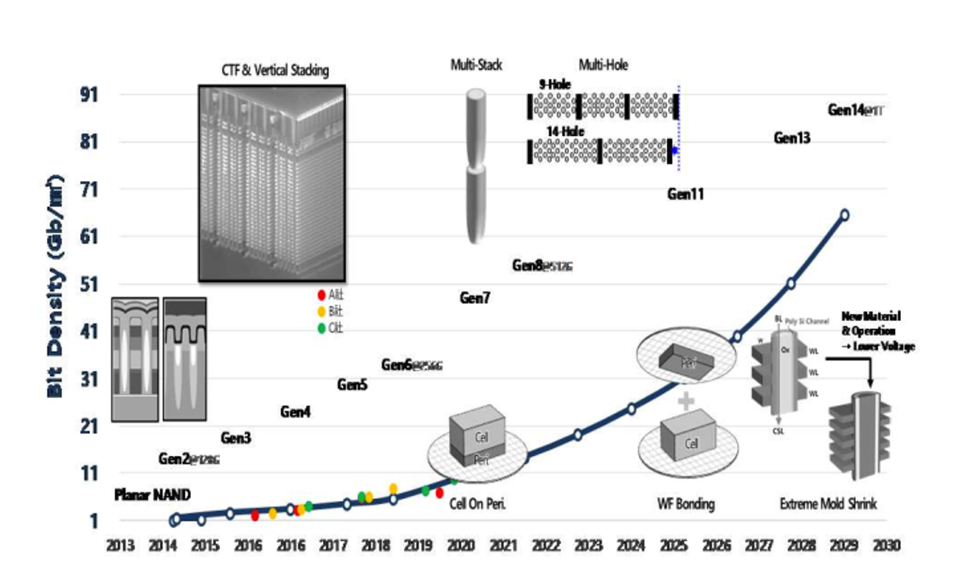
Kim said that current NAND flash bit density is approximately 10 Gb/mm2, and the number of layers stacked increasing to 170 (Fig. 8). Samsung Electronics, expects that cost effective manufacturing of V-NAND with over 1,000 stack layers can be achieved via innovations in next generation processes and novel materials. For next generation V-NAND, the HARC (high aspect ratio contact) etching process and the cell current in VNAND architecture are critical. Stack height will be addressed with multi-stacking and new processes and materials are needed to improve the NAND flash memory signals with smaller stacked cells.
The following figure shows Samsung’s projections for advances in multi-bit cells, new materials and architectures and better cell control.

Innovations in control circuitry, which will minimize Vt spread, and novel materials for charge trap layers, are key innovations. To meet I/O bandwidth requirements, which are expected to double every three years, greater efforts to address thermal effects are needed. A wafer-bonding process, as an example, that decouples process thermal budget for memory cells and peripheral transistors is one way to accomplish this.
Michael Abrash from Facebook Reality labs Research gave a plenary talk on “Creating the Future: Augmented Reality, the next Human-Machine Interface”. He explored developments in virtual reality (VR) and augmented reality (AR), collectively called XR that are in use today and developments that could enable future more immersive experiences and replace devices such as smart phones with wearable technologies, such as AR glasses.
Making such devices possible will require new sensor technology, software (including ways to map and understand that world that incorporate personal contextual information including historical interactions with this mapped representational world), as well as new ways to package electronics with advanced low power processing capabilities.
These advanced low power and miniaturized packages will require innovations on hardware and software do-design, heterogeneous package integration and miniaturization as shown in the figure below. Note in particular the mention of memory-centric computing under HW-SW Co-Design and eNVMs in the miniaturization area to achieve comfortable, useful AR/VR devices.

Abrash mentioned the possible use of spintronics, 2D materials, carbon nano tubes (CNRTs), functional interconnects, flexible and meta-materials) to enable higher system performance a lower unit power density and smaller physical volume to enable these wearable future devices.
He also mentioned the need to develop new architectures and domain-oriented accelerations to support machine learning (ML) but also for particular applications such as avatar tracking and reconstruction, audio, eye tracking and electromyography with wearable sensors on the users arms. Algorithmic optimization will be needed for model compression, low precision computing and platform-aware design optimization.
Current AR/VR computing systems consumer the most power in data transfers and memory access. On-sensor computing and memory-centric computing approaches such as compute-in-memory will be needed to tackle these bottlenecks. In addition, tighter physical coupling of logic with memories, logic with sensors and displays can help reduce data movement. He also mentioned the importance of using embedded non-volatile memories like spin transfor torque magnetic random-access memories (STT-MRAM) will be important in achieving power and area optimization since these memories have higher density that SRAM and are non-volatile, allowing more lower power states.
He talked about advances in image sensors that include the use of a hybrid memory hierarchy (including SRAM and eNVM, such as MRAM) in on-sensor ML computation architecture to allow for higher density and lower power. 3DIC technologies, such as three-layer stacking, through silicon vias (TSVs) and wafer-level hybrid bonding, will enable this heterogeneous monolithic integration. The figure below shows a multi-camera AR/VR distributed multi-camera computing system with various features, including the use of the hybrid memory systems. The figure also indicates the energy and communication requirements for the various computing/communication paths.

At the 2021 IEEE IEDM Samsung spoke about expected developments in DRAM and NAND technology out to 2030 to enable advanced electronics. Facebook spoke about requirements, including in-memory computing and emerging memories such as MRAM to enable future comfortable wearable AR/VR devices that will enable new ways to work and interact with other and the world around us.