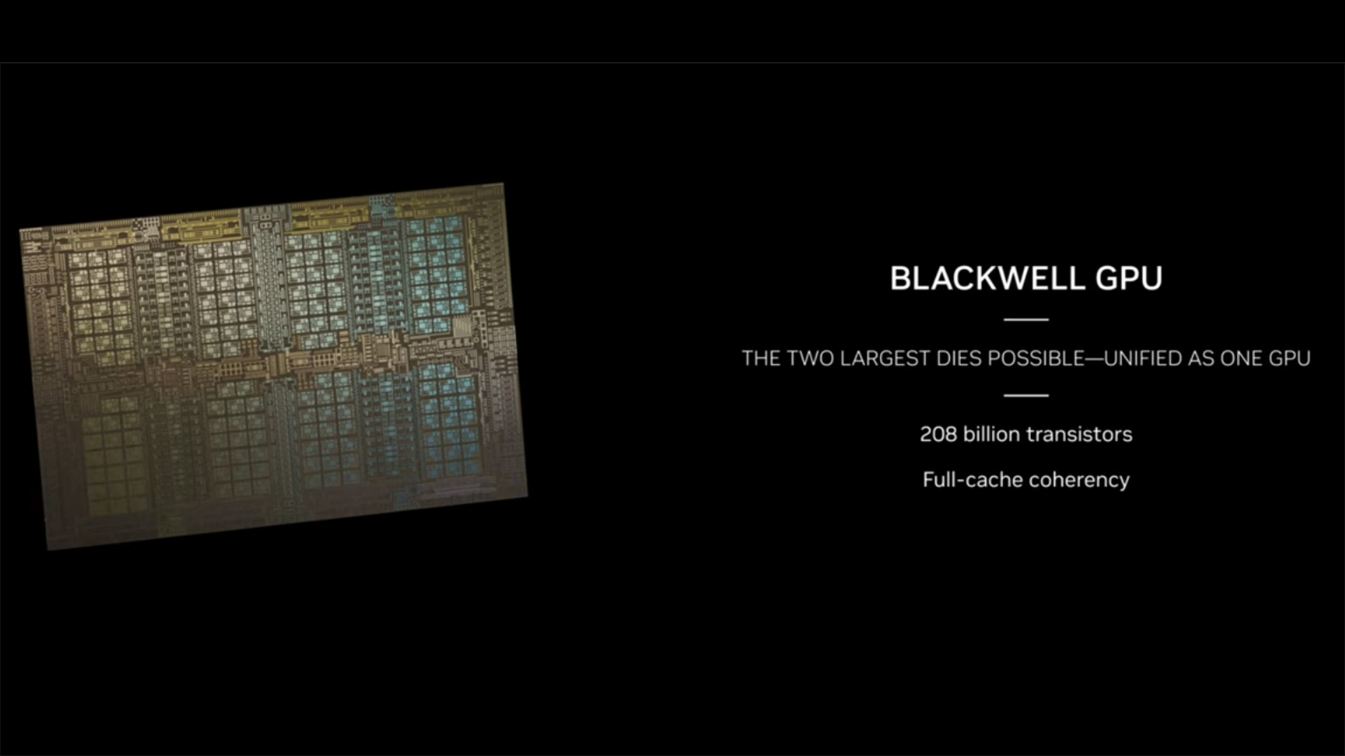
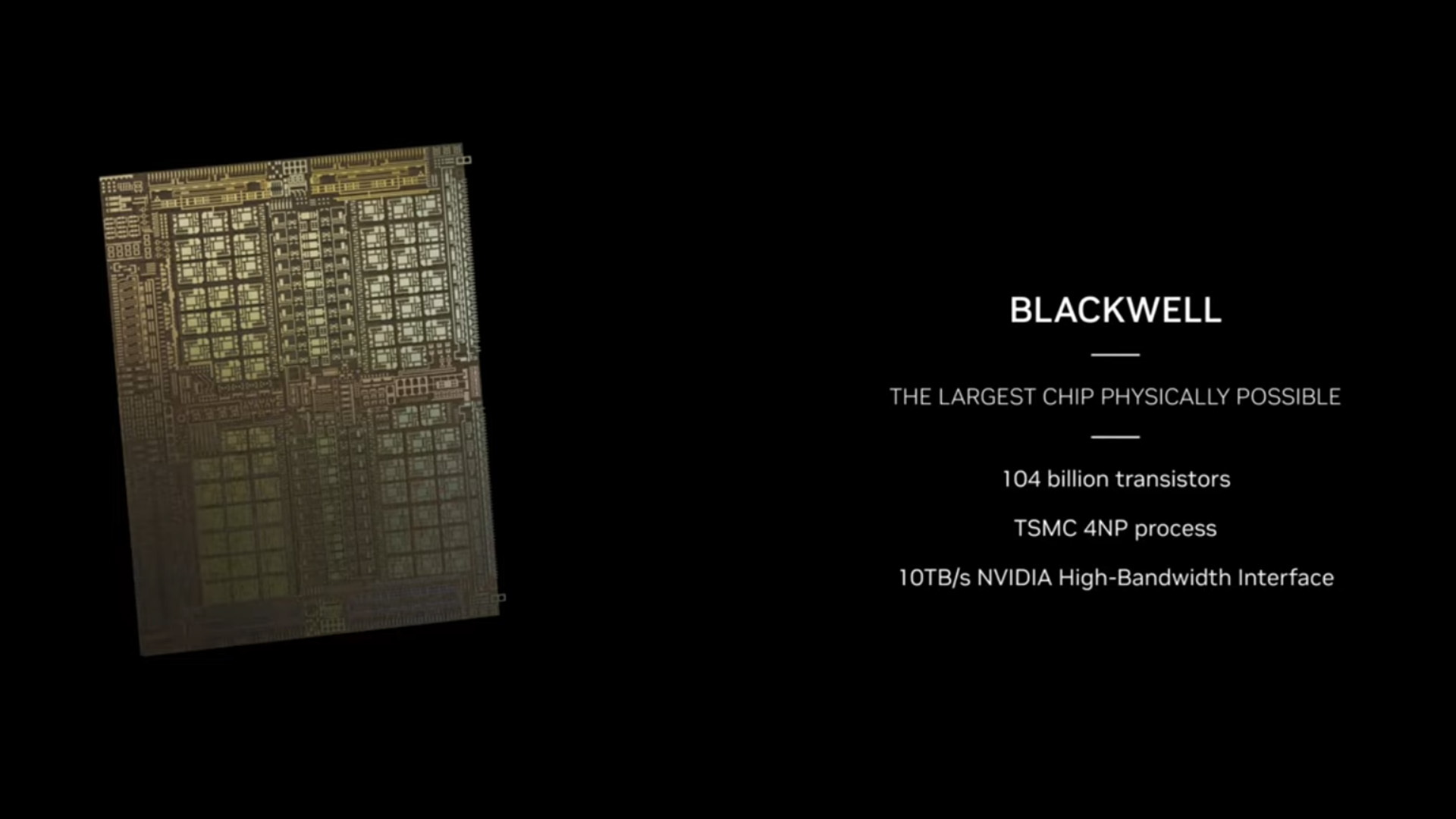
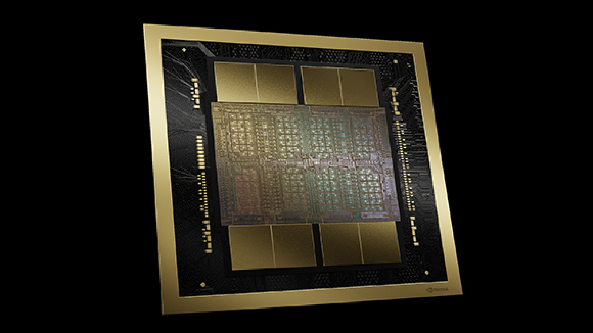
There's a new Nvidia architecture in town, and it's a doozy. Blackwell has just been announced by Nvidia's CEO Jensen Huang at GTC and will feature inside the ludicrously large B200 GPU. To call them 'GPUs' would technically be wrong, however. They're dual-GPU packages with a total of 208 billion transistors across them. To put that into perspective, the previous must-have compute chips out of Nvidia, the Hopper H200 and H100, has just over 80 billion transistors. An RTX 4090 has 76.3 million. We're looking at over double that with Blackwell, which makes a lot of sense considering it's dual-wielding GPUs and a new chip-to-chip interconnect.
Blackwell is unfortunately not for gaming. Boo! I'm not sure our bank accounts would be ready for such a mighty thing anyways. Blackwell is mostly intended for rollout within data centres chasing bigger and bigger compute figures. Why? Artificial intelligence, mostly.
But since we're awaiting any news on the next-generation GeForce graphics cards, let's keep in mind which features might end up being transplanted from these mahoosive Blackwell chips into whatever architecture turns up in the next graphics cards for gaming—which could also be Nvidia Blackwell, albeit a stripped-down version, as we won't need all of the gubbins included with the B200/B100.
Let's start with something we probably will see in a GeForce GPU in future: Blackwell features new fifth-generation Tensor Cores. These are accelerators for instructions largely used within AI applications, i.e. inference and training, and the fifth-gen versions are set to bump performance by up to 30 times. The new Tensor Cores include precision formats and an updated Transformer Engine, which was first introduced with Hopper, to accelerate inference and training of large language models.
Since GeForce cards use Tensor Cores for features such as DLSS, and we've already seen fourth-generation Tensor Cores make the leap from Nvidia's enterprise-only Hopper architecture into the Ada Lovelace architecture powering the RTX 40-series, we're likely to see the same happen with the next-gen. Though how these additional features will be leveraged by Nvidia will be the key thing: a new DLSS version or Frame Generation feature would be the likely candidates for further development.
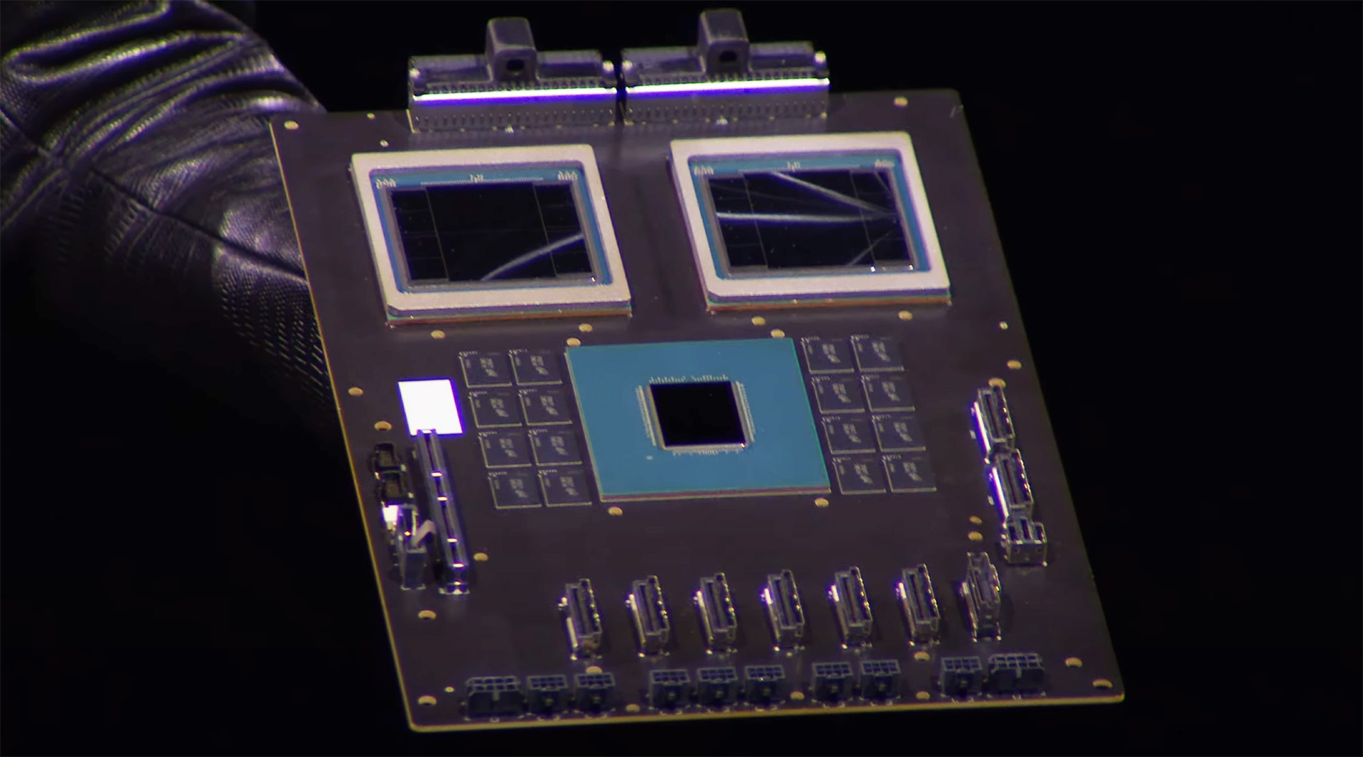
Below: flick through the gallery for a step-by-step of how each part of the Blackwell package comes together.
The Blackwell B200 and B100 both appear cut from the same cloth. The B200 offers higher compute performance within the larger HGX B200 system (made up of eight B200 GPUs) than the B100 does in the HGX B100 system (made up of eight B100 GPUs) at 40TFLOPs FP64 to 30 TFLOPs FP64, but performance appears close enough for us to presume both B200 and B100 built out of the same mammoth 208 billion transistor package.
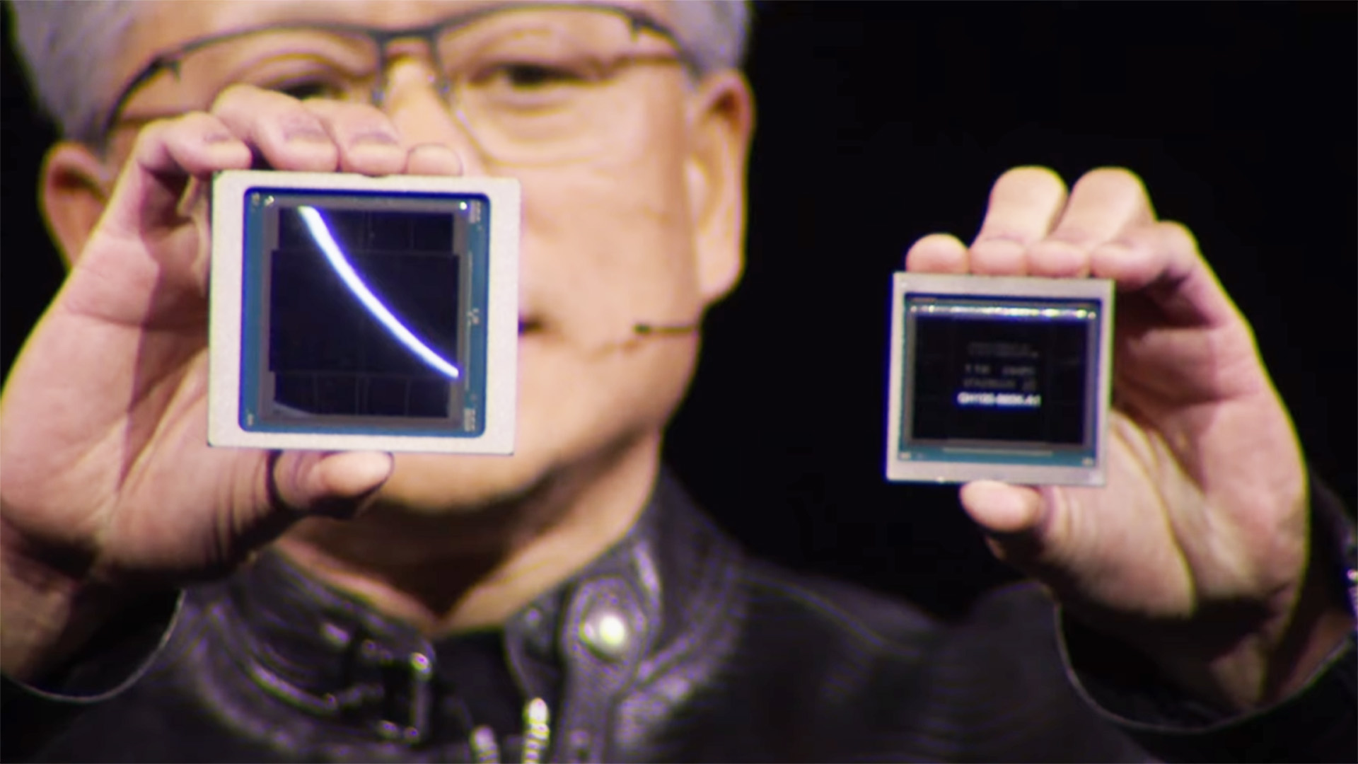
"It's okay, Hopper," says Huang as he holds the gargantuan Blackwell package next to a Hopper die.
The Blackwell chip features two GPUs seen to be acting as a single chip—each GPU built at what's known as the reticle limit, which is essentially the maximum manufacturable size for a single chip in any given lithographic process. As Huang notes during his keynote: "There's a small line between two dies, this is the first time two dies have abutted like this together in such a way that the two dies think it's one chip."
Nvidia has played around with splitting GPUs before. The Ampere GA100 GPU was more or less split down the middle into two halves with an interconnect, though the actual silicon wasn't. Blackwell makes that further leap with two properly sliced silicon halves.
Four years ago, we split GA100 into two halves that communicate through an interconnect. It was a big move - and yet barely anyone noticed, thanks to amazing work from CUDA and the GPU team.Today, that work comes to fruition with the Blackwell launch. Two dies. One awesome GPU. https://t.co/XuaUQPskkM pic.twitter.com/svRKhwPYEnMarch 18, 2024
Will the same dual-GPU design make it into a gaming graphics card? It's pretty darn unlikely but not altogether impossible.
For starters, leaks suggest the biggest graphics card in the next-generation Nvidia lineup, presumably the RTX 5090, will come with many more CUDA Cores than its predecessor, the RTX 4090. Though current rumours don't suggest any sort of direct doubling of the RTX 4090 spec. Even if the RTX 5090 were using two smaller GPUs to make for a more efficient chip, there are more concrete reasons why a dual-GPU approach could be unrealistically tricky.
Getting two GPUs to run as one while gaming is enormously tough—that's why CrossFire and SLI are dead. For this multi-GPU approach to work the two GPUs would need to act as one while necessitating next to no changes to the APIs that communicate with a graphics card.
Huang does note that "these two sides of the Blackwell chip have no idea which side they're on," in reference to how the Blackwell GPU package works together as one. "There's no memory locality issues, no cache issues. It's just one giant chip," Huang continues.
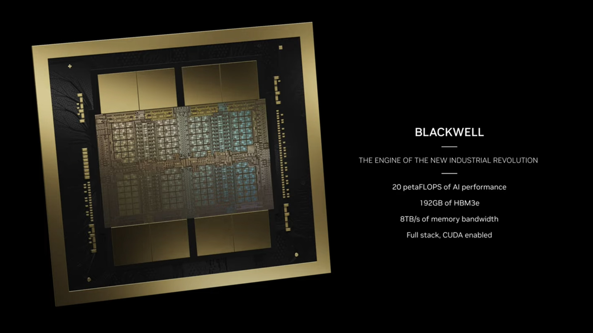
That does fill me with some hope of reaching a point where multi-GPU gaming dies are a possibility, but that's still a tough cookie to crack. It's easier to do with compute chips, such as the B200, provided there's plenty of bandwidth between the two dies—hence why there's a 10TB/s interconnect on the Blackwell GPU.
For now I think it more likely an up-to-date process node will be the primary way Nvidia goes about cramming more cores into a gaming chip. And that's one area where Blackwell offers some indication of what to expect.
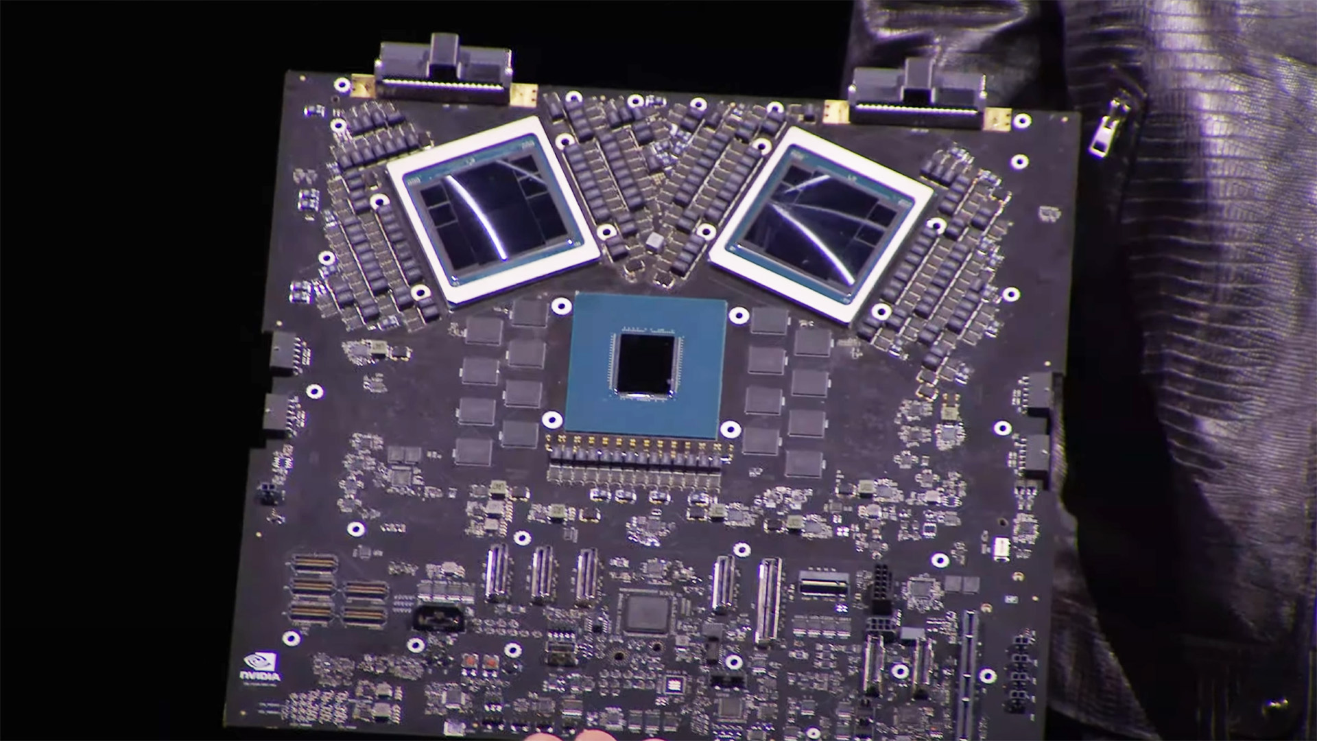
Above: Nvidia has prototype boards for some seriously powerful (and expensive) systems using Blackwell.
What we might see make the leap from Blackwell into a next-gen gaming card is the use of TSMC's 4NP process node. This is reportedly an extension of the custom 4N process node created for and used exclusively by Nvidia's Ada Blackwell and Hopper chips. It's not really a 4nm process node, however, being more closely related to TSMC's 5nm node. It's confusing but that's seemingly by design as almost every major semiconductor manufacturer does the same thing. For example, Intel 7 is actually its 10nm process, and what makes a process 10nm anyways? We could be here a while. Point is, it's very likely we'll see the next-gen GeForce cards using the 4NP process, too.
The Decompression Engine on Blackwell is something of particular interest to gamers. Nvidia introduced RTX IO back in 2020 as a way to shift load from the CPU onto the GPU to speed up game asset load times. It's a part of a wider industry push to integrate GPU decompression into games including AMD's SmartAccess Storage, Microsoft's DirectStorage, and Khronos Group's Vulkan API. They all rely on an open GPU compression standard called GDeflate.
Blackwell's new Decompression Engine specifically accelerates GDeflate specifically, among other decompression standards, and that could come in handy for a wider push to adopt GDeflate in games if it were to also be integrated into next-gen GeForce GPUs. The faster a GPU can decompress assets, the faster they can be loaded into a game, and that means more detailed game worlds can be designed with a reasonable expectation of performance.
Best CPU for gaming: The top chips from Intel and AMD.
Best gaming motherboard: The right boards.
Best graphics card: Your perfect pixel-pusher awaits.
Best SSD for gaming: Get into the game ahead of the rest.
Now there are a few parts of Blackwell unlikely to make it into a future gaming GPU. The Reliability, Availability, and Serviceability (RAS) engine built to identify and report on faults or potential faults before they occur. That's a feature much handier if, like Meta, you're running hundreds of thousands of these things at once. Similarly, the focus on the TEE-I/O security model for "secure AI" won't be necessarily on the agenda for GeForce. The ability to hook up heaps of GPUs together into one superchip or many superchips into one super-system using NVLink will also get thrown on the sacrificial pyre of gaming.
Lastly, we won't see hundreds of gigabytes of HBM3e memory on any RTX 50-series or similar gaming chip. Nvidia's Grace Blackwell Superchip, which incorporates two Blackwell GPUs and a Grace CPU, looks awesome (and expensive) with 384 GB of HBM3e memory offering 16 TB/s bandwidth, but we'll most likely be gaming on 8GB or more (hopefully a lot more) of GDDR7 memory.
A couple of potential graphics goodies from Blackwell that might make the leap into a gaming graphics card, then, and a few more that probably won't. Unfortunately we don't know when we might find out for certain. Nvidia hasn't yet given us a firm date for when next-gen gaming graphics cards will arrive. Nor when products based on Blackwell will arrive, for that matter. The company has little need to advertise, however: Meta, Google, Microsoft, OpenAI, Oracle, xAI, Dell and Amazon are among its clients already lining up for a bit of Blackwell.
If last generation's launch cadence is to be followed, which had Hopper announced in March and Ada Lovelace in September, then we may hear more on next-gen GeForce graphics cards shortly after summer.