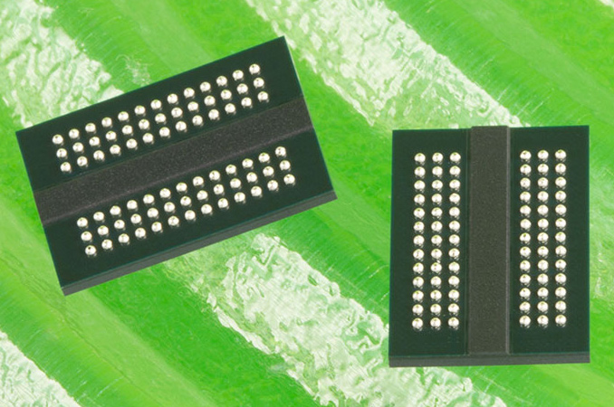
When Samsung teased the ongoing development of GDDR7 memory last October, the company did not disclose any other technical details of the incoming specification. But Cadence recently introduced the industry's first verification solution for GDDR7 memory, and in the process has revealed a fair bit of additional details about the technology. As it turns out, GDDR7 memory will use PAM3 as well as NRZ signaling and will support a number of other features, with a goal of hitting data rates as high as 36 Gbps per pin.
A Short GDDR History Lesson
At a high level, the evolution of GDDR memory in the recent years has been rather straightforward: newer memory iterations boosted signaling rates, increased burst sizes to keep up with those signaling rates, and improved channel utilization. But none of this substantially increased the internal clocks of the memory cells. For example, GDDR5X and then GDDR6 increased their burst size to 16 bytes, and then switched to dual-channel 32-byte access granularity. While not without its challenges in each generation of technology, ultimately the industry players have been able to crank up the frequency of the memory bus with each version of GDDR to keep the performance increases coming.
But even "simple" frequency increases are increasingly becoming not so simple. And this has driven the industry to look at solutions other than cranking up the clocks.
With GDDR6X, Micron and NVIDIA replaced traditional non-return-to-zero (NRZ/PAM2) encoding with four-level pulse amplitude modulation (PAM4) encoding. PAM4 increases the effective data transmission rate to two data bits per cycle using four signal levels, thus enabling higher data transfer rates. In practice, because GDDR6X has a burst length of 8 bytes (BL8) when it operates in PAM4 mode, it is not faster than GDDR6 at the same data rate (or rather, signaling rate), but rather is designed to be able to reach higher data rates than what GDDR6 can easily accomplish.
Four-level pulse amplitude modulation has an advantage over NRZ when it comes to signal loss. Since PAM4 requires half the baud rate of NRZ signaling for a given data rate, the signal losses incurred are significantly reduced. As higher frequency signals degrade more quickly as they travel through a wire/trace - and memory traces are relatively long distances by digital logic standards - being able to operate at what's essentially a lower frequency bus makes some of the engineering and trace routing easier, ultimately enabling higher data rates.
The trade-off is that PAM4 signaling in general is more sensitive to random and induced noise; in exchange for a lower frequency signal, you have to be able to correctly identify twice as many states. In practice, this leads to a higher bit error rate at a given frequency. To reduce BER, equalization at the Rx end and pre-compensation at the Tx end have to be implemented, which increases power consumption. And while it's not used in GDDR6X memory, at higher frequencies (e.g. PCIe 6.0), forward-error correction (FEC) is a practical requirement as well.
And, of course, GDDR6X memory subsystems require an all-new memory controllers, as well as a brand-new physical interface (PHY) both for processors and memory chips. These complex implementations are to a large degree the main reasons why four-level coding has, until very recently, been almost exclusively used for high-end datacenter networking, where the margins are there to support using such cutting-edge technology.
GDDR7: PAM3 Encoding for Up to 36 Gbps/pin
Given the trade-offs mentioned above in going with either PAM4 signaling or NRZ signaling, it turns out that the JEDEC members behind the GDDR7 memory standard are instead taking something of a compromise position. Rather than using PAM4, GDDR7 memory is set to use PAM3 encoding for high-speed transmissions.
As the name suggests, PAM3 is something that sits between NRZ/PAM2 and PAM4, using three-level pulse amplitude modulation (-1, 0, +1) signaling, which allows it to transmit 1.5 bits per cycle (or rather 3 bits over two cycles). PAM3 offers higher data transmission rate per cycle than NRZ – reducing the need to move to higher memory bus frequencies and the signal loss challenges those entail – all the while requiring a laxer signal-to-noise ratio than PAM4. In general, GDDR7 promises higher performance than GDDR6 as well as lower power consumption and implementation costs than GDDR6X.
And for those keeping score, this is actually the second major consumer technology we've seen introduced that uses PAM3. USB4 v2 (aka 80Gbps USB) is also using PAM3 for similar technical reasons. To quote from our initial coverage back in 2021:
So what on earth in PAM3?
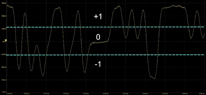
PAM3 is a technology where the data line can carry either a -1, a 0, or a +1. What the system does is actually combine two PAM3 transmits into a 3-bit data signal, such as 000 is an -1 followed by a -1. This gets complex, so here is a table:
| PAM3 Encoding | ||
| AnandTech | Transmit 1 |
Transmit 2 |
| 000 | -1 | -1 |
| 001 | -1 | 0 |
| 010 | -1 | 1 |
| 011 | 0 | -1 |
| 100 | 0 | 1 |
| 101 | 1 | -1 |
| 110 | 1 | 0 |
| 111 | 1 | 1 |
| Unused | 0 | 0 |
When we compare NRZ to PAM3 and PAM4, we can see the rate of data transfer for PAM3 is in the middle of NRZ and PAM4. The reason why PAM3 is being used in this case is to achieve that higher bandwidth without the extra limitations that PAM4 requires to be enabled.
| NRZ vs PAM-3 vs PAM4 | |||
| AnandTech | Bits | Cycles | Bits Per Cycle |
| NRZ | 1 | 1 | 1 |
| PAM-3 | 3 | 2 | 1.5 |
| PAM-4 | 2 | 1 | 2 |
With that said,It remains to be seen how much power a 256-bit memory subsystem with the 36 Gbps data transfer rate promised by Samsung will use. The GDDR7 spec itself has yet to be ratified, and the hardware itself is still being constructed (which is where tools like Cadence's come in). But keeping in mind how bandwidth hungry applications for AI, HPC, and graphics are, that bandwidth will always be welcome.
Optimizing Efficiency and Power Consumption
In addition to increased throughput, GDDR7 is expected to feature a number of ways to optimize memory efficiency and power consumption. In particular, GDDR7 will support four different read clock (RCK) modes in a bid to enable it only when needed:
- Always running: Always running and stops during sleep modes;
- Disable: Stops running;
- Start with RCK Start command: Host can start RCK by issuing the RCK Start command before reading out dataand stop using the RCK Stop command when needed.
- Start with Read: RCK automatically starts running when DRAM receives any command which involves reading data out. It can be stopped using the RCK Stop command.
In addition, GDDR7 memory subsystems will be able to issue two independent commands in parallel. For example, Bank X can be refreshed by issuing a Refresh per bank command on CA[2:0], while Bank Y can be read by issuing a read command on CA[4:3] at the same time. Also, GDDR7 will support linear-feedback shift register (LFSR) data training mode to determine appropriate voltage levels and timings to ensure consistent data transfers. In this mode, the host will keep track of each individual eye (connection), which will allow it to apply appropriate voltages to better optimize power consumption.
Finally, GDDR7 will be able to shift between PAM3 encoding and NRZ encoding modes based on bandwidth needs. In high bandwidth scenarios, PAM3 will be used, while in low bandwidth scenarios the memory and memory controllers can shift down to more energy efficient NRZ.
Cadence Delivers First GDDR7 Verification Solution
While JEDEC has not formally published the GDDR7 specification, this latest technical data dump comes as Cadence has launched their verification solution for GDDR7 memory devices. Their solution fully supports PAM3 simulation by a real number representation, it supports binary bus, strength modeling, and real number modeling.
The verification IP also supports various modes of error injection in multiple fields of transactions during array data transfer and interface trainings. Furthermore, it comes with the waveform debugger solution to visualize transactions on the waveform viewers for faster debugging and verification.
"With the first-to-market availability of the Cadence GDDR7 VIP, early adopters can start working with the latest specification immediately, ensuring compliance with the standard and achieving the fastest path to IP and SoC verification closure," a statement by Cadence reads.
When Will GDDR7 Land?
While GDDR7 promises major performance increases without major increases of power consumption, perhaps the biggest question from technical audiences is when the new type of memory is set to become available. Absent a hard commitment from JEDEC, there isn't a specific timeframe to expect GDDR7 to be released. But given the work involved and the release of a verification system from Cadence, it would not be unreasonable to expect GDDR7 to enter the scene along with next generation of GPUs from AMD and NVIDIA. Keeping in mind that these two companies tend to introduce new GPU architectures in a roughly two-year cadence, that would mean we start seeing GDDR7 show up on devices later on in 2024.
Of course, given that there are so many AI and HPC companies working on bandwidth hungry products these days, it is possible that one or two of them release solutions relying on GDDR7 memory sooner. But mass adoption of GDDR7 will almost certainly coincide with the ramp of AMD's and NVIDIA's next-generation graphics boards.