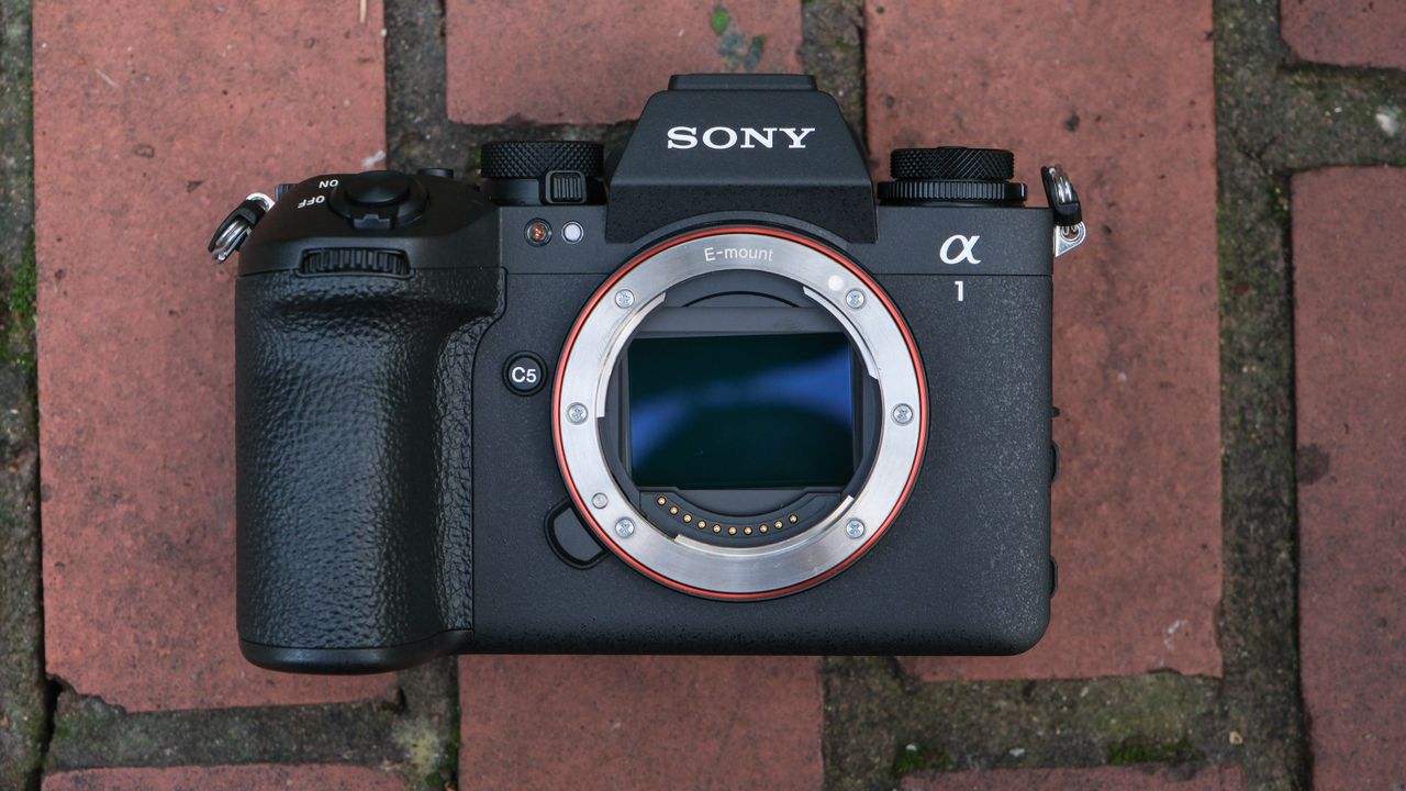
Sony’s design for a stacked sensor brought faster shooting speeds to both smartphones and mirrorless cameras – but a new presentation suggests that the company is researching the possibility of adding a third layer.
In a presentation shared with investors earlier this year, president and CEO of Sony Semiconductor Solutions Corporation, Shinji Sahsida, shared a company outlook that includes evolving Sony’s stacked sensor technology to include an additional layer.
[Editor's note: Last year a patent was spotted from Canon, which is designing a triple-stacked sensor of its own.]
In the presentation, Sony shared a three-layer sensor design that sandwiches an “⍺” layer in-between the existing pixel and logic layers in the two-layer design.
“Specifically, it is three-layer stacking technology that evolves our strength in stacking technology,” Sahsida said during the presentation. “Different functions can be layered between the conventional pixels and logic to further enhance characteristics.”
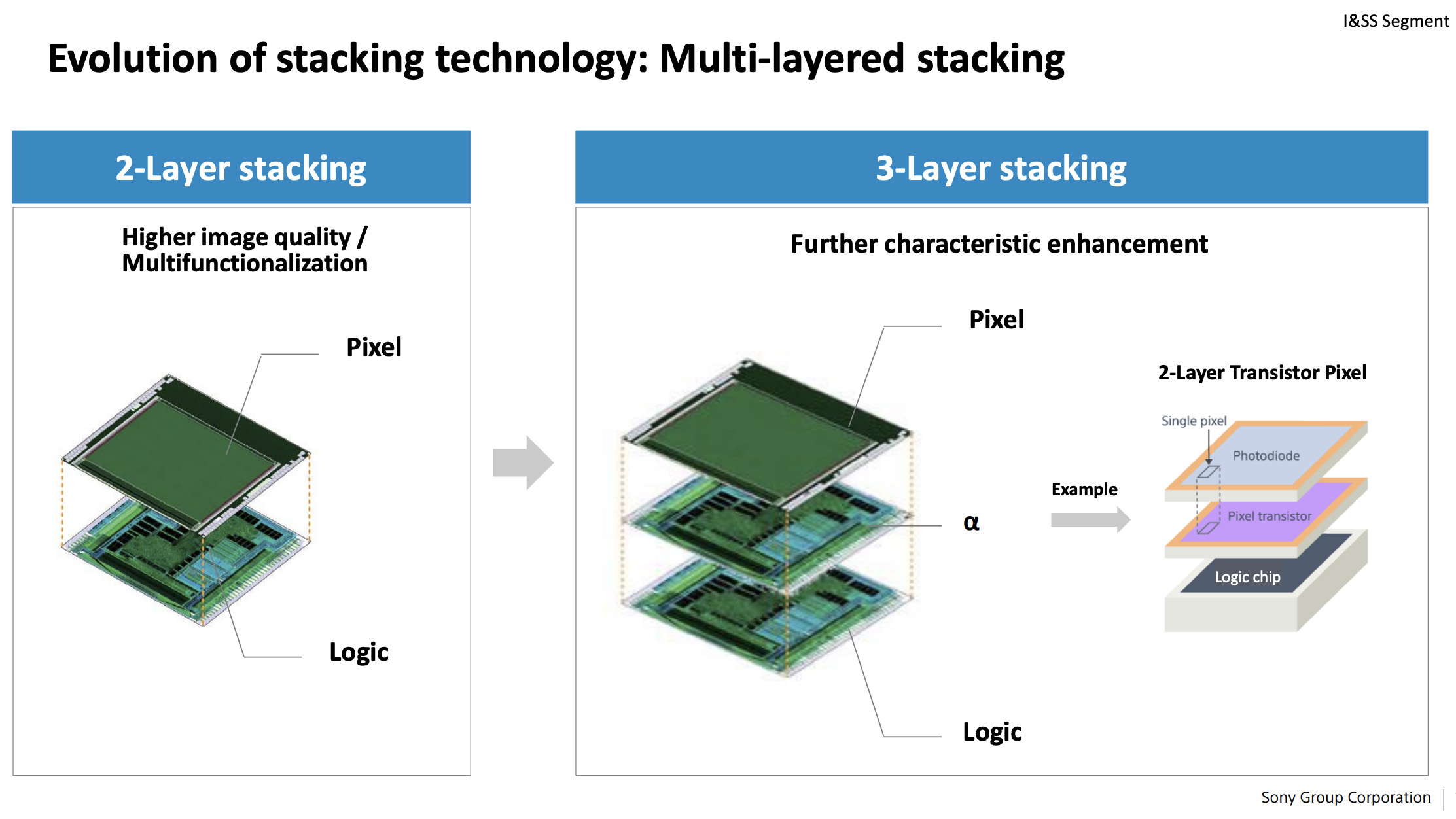
“In addition to this, we expect various possibilities to come from the combination of three layers, and we believe that three-layer stacking will be an important axis for technological evolution in the future.”
Sony then explained that the benefits of that three-layer design would include a wider dynamic range, without blowouts in bright scenes and while keeping noise in the shadows low. Resolution, readout speeds and power consumption would also benefit.
The company listed those benefits across both camera phones and interchangeable lens mirrorless cameras, as well as some improvements across both stills and video.
Sony indicates that both layering and process node adjustments are integral to achieving higher density sensors (which often refers to a higher pixel density, or higher resolution) as well as the realization of “2D + XD”.
The creator of Sony’s stacked CMOS sensor, Taku Umebayashi, once explained where the idea for the two-layered sensor came from. “While the pixel section is the heart of an image sensor, I as a specialist of logic circuit, saw it like a sore spot that got in the way of the logic circuit,” he said in an interview from 2022.
“I thought that it might work well if the components were separated and then put together after their processes were formed. In this way, both parts could fully leverage their respective advantages. Stacking the pixel section on the logic circuit section would result in a smaller chip size, and therefore, the productivity per wafer would improve, which would realize a 'cheaper' sensor and solve the problem.”
As part of the presentation for the company’s mid to long-term business direction, it’s unclear when the three-layer design could potentially make it out to consumer devices, nor is it clear exactly what that third “⍺” layer entails.
But Sony’s existing stacked sensor has brought with it a number of advantages, and it’s a glimpse into what Sony’s sensor development company is imagining for the future.
You may also like
Browse the best Sony cameras or the best smartphones for photography.