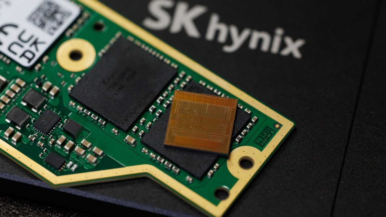
SK hynix announced iHBM today, a memory heat management technology designed to enhance AI system performance. The thermal packaging solution improves heat dissipation by integrating ICEs (integrated cooling elements) directly into the HBM package. SK hynix says the result is an over 30% reduction in thermal resistance, “ensuring stable operating characteristics even in high-temperature and high-load environments.”
Go deeper with TH Premium: Memory
- AI data centers are swallowing the world's memory and storage supply
- The future of DRAM: From DDR5 to future ICs
- High-bandwidth memory roadmap
- Here's why HBM is coming for your PC's RAM
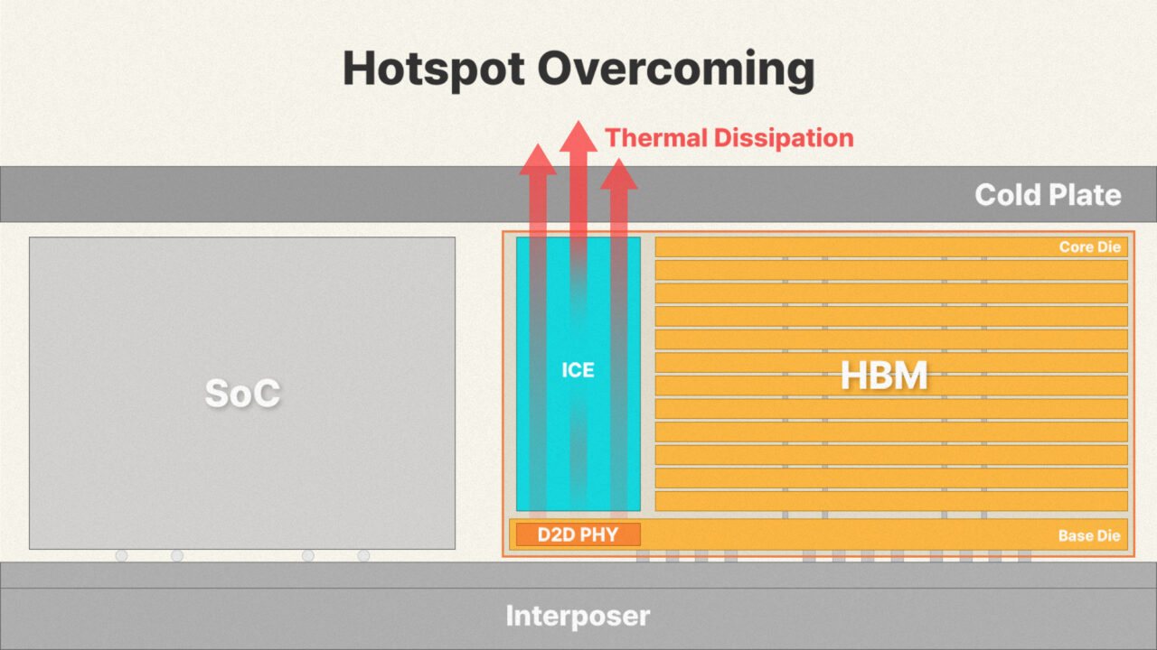
The iHBM architecture embeds non-conductive silicon cooling elements directly into the Die-to-Die Physical Layer (D2D PHY), the critical, high-speed connection interface between the HBM base die and the AI processor, which is prone to high temperature spikes as a result of extreme data traffic. By placing cooling elements in this layer, SK hynix mitigates the severe thermal throttling that cripples AI system performance during heavy computational workloads.
The company believes that structurally preventing thermal throttling will enable next-generation memory layers (targeted for future generations like HBM5) to scale to higher stack heights and sustain maximum data transfer speeds under the heavy computational loads of AI data centers.
“iHBM is the optimal solution for minimizing heat generation developed by combining memory design capabilities and advanced packaging technology,” said SK hynix Vice President Lee Kang-wook. “We will proactively provide the value customers need in the AI environment and further solidify our leadership in AI memory.”
SK hynix plans to apply iHBM technology from next-generation products, such as HBM5, to meet the thermal management requirements of high-performance computing (HPC), AI data centers, and other ultra-high-density and ultra-high-bandwidth environments, thereby improving overall system stability and efficiency.
Heat management is one of the biggest challenges facing HBM (High-Bandwidth Memory) technology. Unlike conventional memory, HBM achieves massive bandwidth by vertically stacking multiple DRAM dies, dramatically shortening the distance data must travel and enabling far higher transfer speeds with better power efficiency.
To minimize latency and feed AI processors fast enough to avoid bottlenecks, HBM is placed extremely close to the GPU or AI accelerator on the same package, connected through a high-speed silicon interposer. However, this dense arrangement also creates severe thermal problems.
The Die-to-Die Physical Layer (D2D PHY) — the ultra-high-speed interface linking the processor and HBM stacks — continuously moves terabytes of data per second. As thousands of signaling lanes and billions of transistors switch at extremely high frequencies, switching losses, leakage current, and electrical resistance generate substantial heat.
The problem is compounded by the processor itself, which already produces enormous amounts of heat. With the HBM stacks packed tightly around the processor, heat accumulates rapidly in a very small area. When temperatures exceed safe limits, the system automatically reduces clock speeds and voltages through thermal throttling to prevent physical damage, lowering overall performance.
SK hynix's new iHBM approach attempts to tackle the problem at the structural level. Unlike conventional HBM cooling designs that primarily dissipate heat indirectly through the core die and surrounding package structures, the company's iHBM architecture instead places Integrated Cooling Elements (ICEs) directly around the D2D PHY region — the exact zone where thermal concentration is most severe. This approach creates a dedicated dissipation path at the source, reducing overall thermal resistance by 30% and allowing the chip to maintain stable operation under the high-temperature, high-pressure conditions that dense AI workloads demand.
SK hynix says the technology can be manufactured at scale using its existing Wafer Level Packaging (WLP) process, which is built on its Mass Reflow Molded Underfill (MR-MUF) packaging technology already used in commercial HBM products. The design is also architecturally compatible with existing System-in-Package configurations, meaning customers can integrate the new thermal capability without major redesigns.