
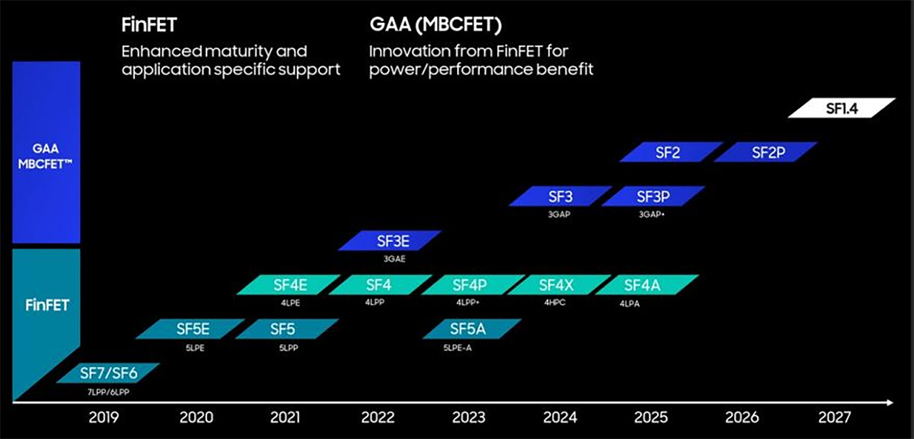
Although Samsung Foundry started to produce chips using its SF3E (aka 3nm gate-all-around early) manufacturing technology last June, the company only uses this tech for select chips, and it's not expected to be used widely. Meanwhile, the company is working on its second-gen 3nm-class node called SF3 (3GAP) and will disclose more information about it at the upcoming 2023 Symposium on VLSI Technology and Circuits in Kyoto, Japan.
Samsung's Sf3 (3nm-class) fabrication technology (set to be introduced at the T1-2 session) will use the company's second-gen Multi-Bridge-Channel field-effect transistors (MBCFET). This new fabrication technology builds upon the first-gen GAA device (SF3E) that's already in mass production, incorporating further optimization.
Samsung claims that compared to SF4 (4LPP, 4nm-class, low power plus), SF3 offers a 22% higher performance at the same power and transistor count, a 34% power reduction at the same clocks and complexity, and a 0.79x logic area reduction. However, Samsung doesn't compare its SF3 to SF3E, and there is no word about the SRAM and analog circuit scaling.
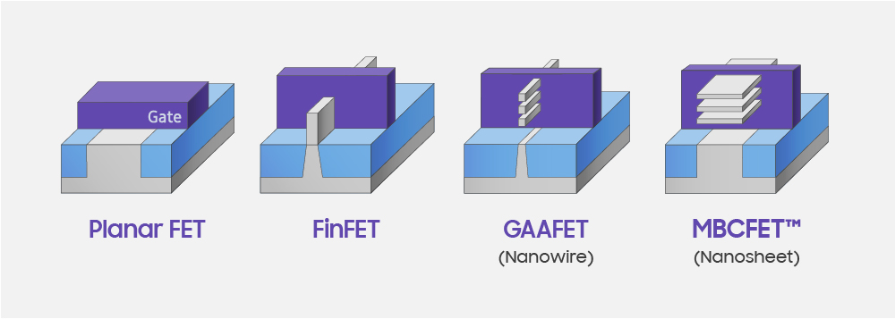
One of the main benefits of GAA transistors over FinFET devices is the reduced leakage current since their gate is surrounded by the channel on all four sides. Additionally, the channel thickness can be adjusted to enhance performance or reduce power consumption.
Samsung now says that the SF3 platform offers greater design flexibility enabled by various nanosheet (NS) widths of the MBCFET device within the same cell type. It is unclear whether it means that the original SF3E lacks one of the key capabilities of GAA transistors, but Samsung's phrasing at least implies it.
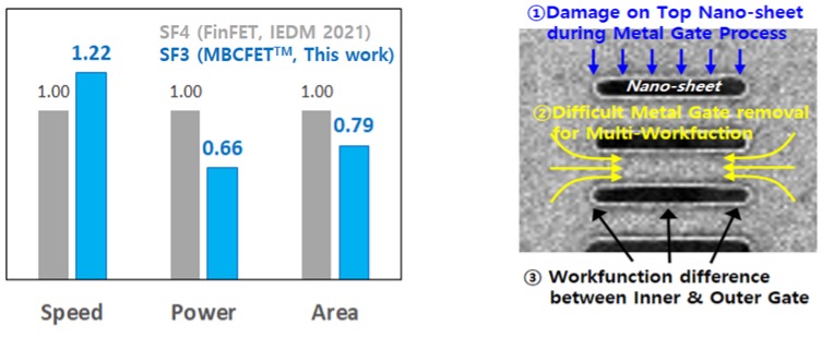
An image that Samsung demonstrates in its paper depicts damage on top of the nanosheet during the metal gate process, so we may speculate that one of the aspects that the company will cover are production challenges it encountered with its GAA-based SF3E production node.
Interestingly, recently the company admitted that its fabrication processes are behind those of TSMC, and it will take at least five years to catch up.
"To be honest, Samsung Electronics' foundry technology lags behind TSMC," said Dr. Kye Hyun Kyung, the head of the Samsung Electronics Device Solutions Division, who is in charge of the company's Memory, System LSI and Foundry business units at a lecture at the Korea Advanced Institute of Science & Technology (KAIST), according to Hankyung (via @Tech_Reve). "We can outperform TSMC within five years."
Samsung Foundry's most advanced fabrication processor for complex SoCs for smartphones and other demanding applications is SF4 (4LPP, 4 nm, low-power plus). However, the company acknowledges that it significantly lags behind TSMC's N3 (N3B) node, which is reportedly used to make some of Apple's sophisticated SoCs. Samsung aims to close the gap with TSMC's N3 and N4P with its SF4P (4LPP+) technology that's expected to be production ready later this year, as per a clarification by @Tech_Reve.
With its SF3 (3GAP), the 2nd generation MBCFET-based node, Samsung Foundry may have better chances to compete against TSMC's leading-edge node in 2024. Also, Samsung intends to offer its SF4X (4HPC), a 4 nm-class fabrication technology designed for high-performance CPUs and GPUs around the same time. However, TSMC is also expected to introduce its performance-enhancing N3P manufacturing technology by then.
Samsung is confident that transitioning to GAA transistors in 2022 – 2023 was a wise move, as it will allow the contract chipmaker to resolve any issues with the new architecture before competitors like Intel and TSMC. Consequently, when these rivals begin producing chips using their 20A, N2 (2nm-class) in 2024-2025 and potentially face similar challenges that Samsung is addressing now, Samsung believes that its SF2 node will provide a superior balance of power, performance, transistor density, costs, and yields.