The tech world has been going wild over AI since we first started hearing about generative language models and the likes. Things have only escalated with more companies adopting AI powered computing, driving demand for capable hardware. We've seen this with Nvidia's AI GPUs coming under hot demand for data centres, and now Samsung appears to be doubling its efforts for this new type of computational processing.
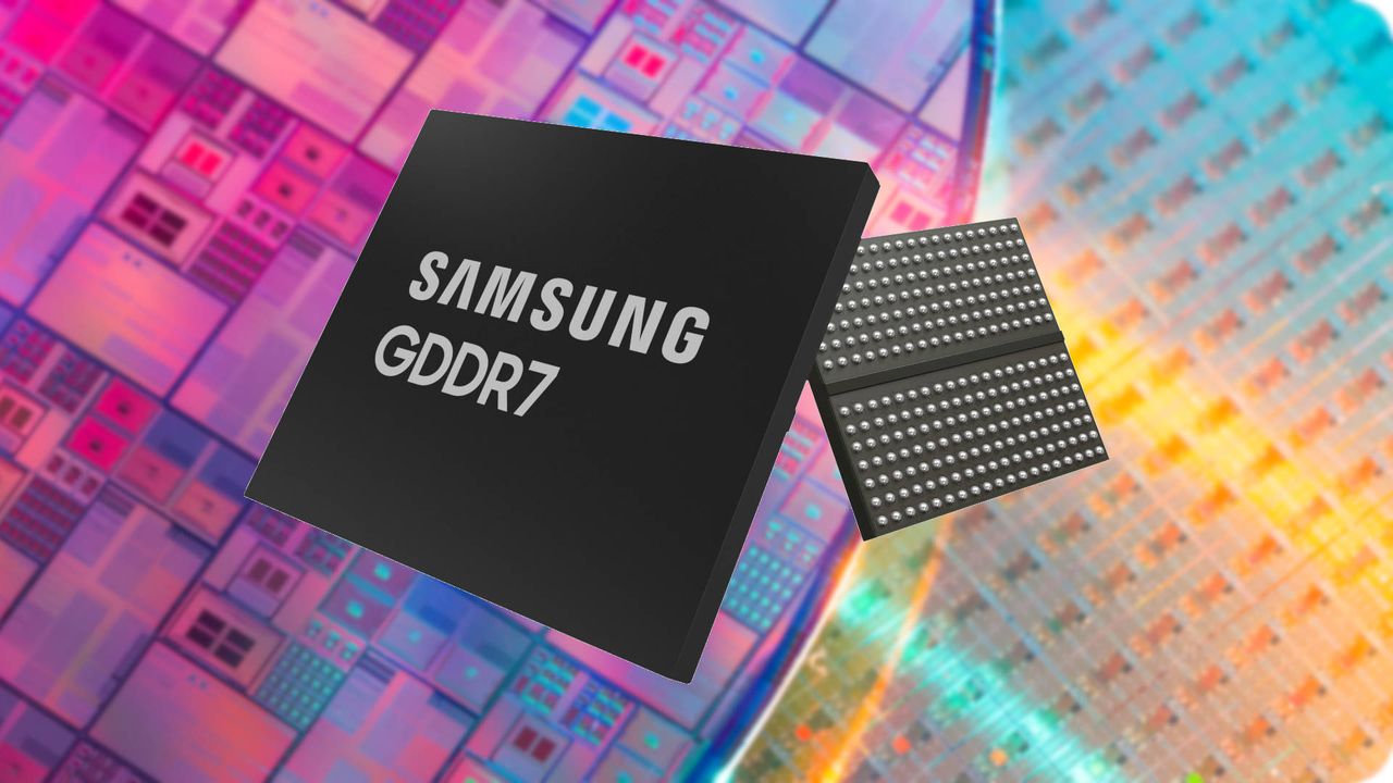
According to The Korea Economic Daily, Samsung has just increased its hiring target for specialists around AI chip development. Specifically the company is after those experienced with high-bandwidth memory or HBM DRAM, and next generation chips. These are important factors for developing AI powered hardware, as AI models are incredibly memory-intensive. They need heaps of the stuff. HBM offers the best way to deliver that memory for datacenter hardware, though attempts to use HBM for gaming graphics cards died a death a while back with AMD's Vega generation.
In an effort to bolster its semiconductor operations, Samsung plans to hire professionals across its memory chip business, foundry, semiconductor research centre, global manufacturing and infrastructure, test and system package, and AI centre. This is on top of spending billions on this just last year. It will also be scaling back hires when it comes to some aspects of its foundry division, further implying a push towards newer technologies.
HBM is a big one of these, with Samsung specifically looking for folks experienced and interested in developing customised HBM. This can mean working to deliver custom dies to forge bespoke chips made of stacked DRAM for customers or functions.
To help with production, Samsung is also looking into Hybrid Bonding technology. This is used to make the processes of building HBM chips much smoother, literally. It allows for chips to be directly connected, rather than having bumps between them which reduces the width of the chip and generates less heat. Having these direct channels allows the chips to access memory in parallel, greatly increasing the efficiency.
Right now we see 12-layer AI HBM chips at the highest tiers like Samsung's HBM3 Icebolt, with companies working towards chips with 16 DRAM layers. Hybrid Bonding is going to be crucial in making this step up to a larger chip while still managing size and heat. Seeing Samsung target these areas definitely gives the impression the company is going to be trying to develop specifically for AI computing in the next few years.
Another pointer to this is what Samsung isn't hiring. The company is to cease hiring in areas developing products like Exynos processors and image sensors. This comes after losses from the division, so it seems the company is looking to pivot from these less profitable technologies into further AI development.
Samsung are a huge electronics company, perhaps best known for its phones but responsible for countless appliances. They have also been fabricators of components, but I don't know if I'd expect much more of this outside of AI directly from the company in the near future.