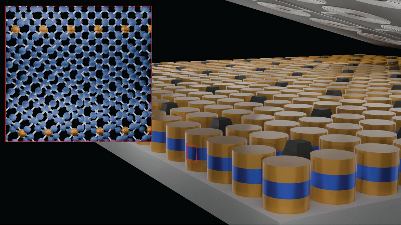
Researchers at NYU and the University of Queensland have demonstrated superconductivity in gallium-doped epitaxial germanium, fabricated using industry-standard semiconductor tools. The new material switches to a superconducting state below 3.5 Kelvin and supports dense, wafer-scale Josephson junction arrays, an important building block for quantum and cryogenic RF circuits.
The team’s prototype demonstrates millions of superconducting junctions integrated on a single 2-inch wafer. Junctions were lithographically defined and electrically characterized at low temperatures, confirming both superconducting behavior and practical current densities for device integration.
The process relies on molecular beam epitaxy to grow ultra-clean germanium films with gallium dopants inserted directly into substitutional lattice sites. At sufficiently high doping concentrations, the films undergo a bulk superconducting transition. Crucially, the interface remains epitaxial and free of disordered interlayers, which are known to degrade junction performance in hybrid stacks.
The work marks a significant shift from small-batch, layered superconductors toward scalable wafer-level integration on semiconductor-grade substrates. Because the doped Ge films are grown using the same epitaxial techniques used in compound semiconductor and cryo-CMOS production, the platform should be theoretically compatible with existing foundry workflows.
Superconducting qubit arrays and cryogenic microwave front-ends today depend on complex packaging steps to integrate semiconducting control logic with superconducting interconnects. Embedding both domains into a monolithic stack removes key bottlenecks in parasitic capacitance, thermal anchoring, and interconnect reliability, which currently limit performance in high-density quantum systems.
The researchers also emphasize the uniformity of their junction fabrication, showing highly consistent critical current densities across large areas. While the transition temperature remains firmly cryogenic, the manufacturability shift opens the door to wider deployment in quantum computing, low-noise detection, and space-based cryo-RF applications.
For now, the focus turns to larger wafers, reproducibility across fabrication nodes, and coupling between superconducting Ge films and conventional on-wafer logic. If follow-up work confirms these properties, superconducting Ge may offer a pragmatic route to scalable quantum interconnects.

Follow Tom's Hardware on Google News, or add us as a preferred source, to get our latest news, analysis, & reviews in your feeds.