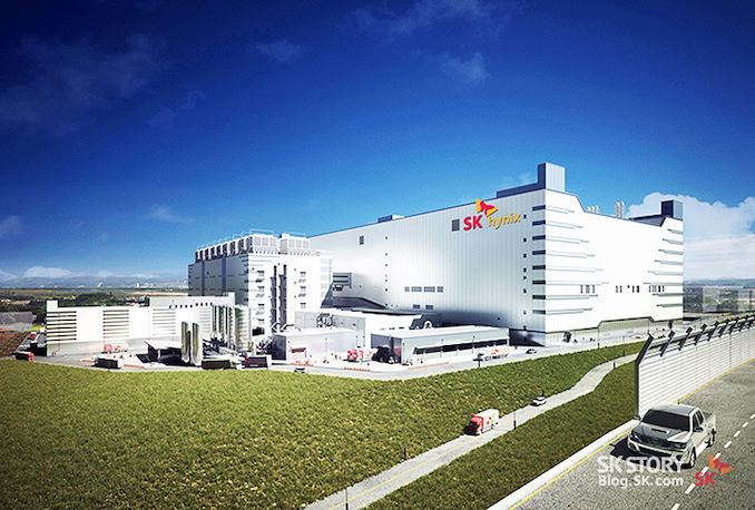
SK hynix is considering whether to build an advanced packaging facility in Indiana, reports the Wall Street Journal. If the company proceeds with the plan, it intends to invest $4 billion in it and construct one of the world's largest advanced packaging facilities. But to accomplish the project, SK hynix expects it will need help from the U.S. government.
Acknowledging the report but stopping short of confirming the company's plans, a company spokeswoman told the WSJ that SK hynix "is reviewing its advanced chip packaging investment in the U.S., but hasn’t made a final decision yet."
Companies like TSMC and Intel spend billions on advanced packaging facilities, but so far, no company has announced a chip packaging plant worth quite as much as SH hynix's $4 billion. The field of advanced packaging – CoWoS, passive silicon interposers, redistribution layers, die-to-die bonding, and other cutting edge technologies – has seen an explosion in demand in the last half-decade. As bandwidth advances with traditional organic packaging are largely played out, chip designers have needed to turn to more complex (and difficult to assemble) technologies in order to wire up an ever larger number of signals at ever-higher transfer rates. Which has turned advanced packaging into a bottleneck for high-end chip and accelerator production, driving a need for additional packaging facilities.
If SK hynix approves the project, the advanced packaging facility is expected to begin operations in 2028 and could create as many as 1,000 jobs. With an estimated cost of $4 billion, the plant is poised to become one of the largest advanced packaging facilities in the world.
Meanwhile, government backing is thought to be essential for investments of this scale, with potential state and federal tax incentives, according to the report. These incentives form part of a broader initiative to bolster the U.S. semiconductor industry and decrease dependence on memory produced in South Korea.
SK hynix is the world's leading producer of HBM memory, and is one of the key HBM suppliers to NVIDIA. Next generations of HBM memory (including HBM4 and HBM4E) will require even closer collaboration between chip designers, chipmakers, and memory makers. Therefore, packaging HBM in America could be a significant benefit for NVIDIA, AMD, and other U.S. chipmakers.
Investing in the Indiana facility will be a strategic move by SK hynix to enhance its advanced chip packaging capabilities in general and demonstrating dedication to the U.S. semiconductor industry.