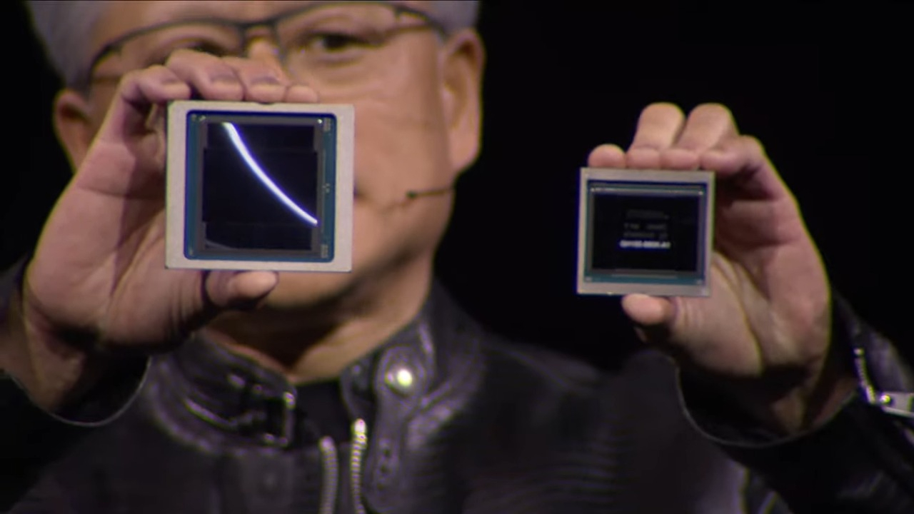
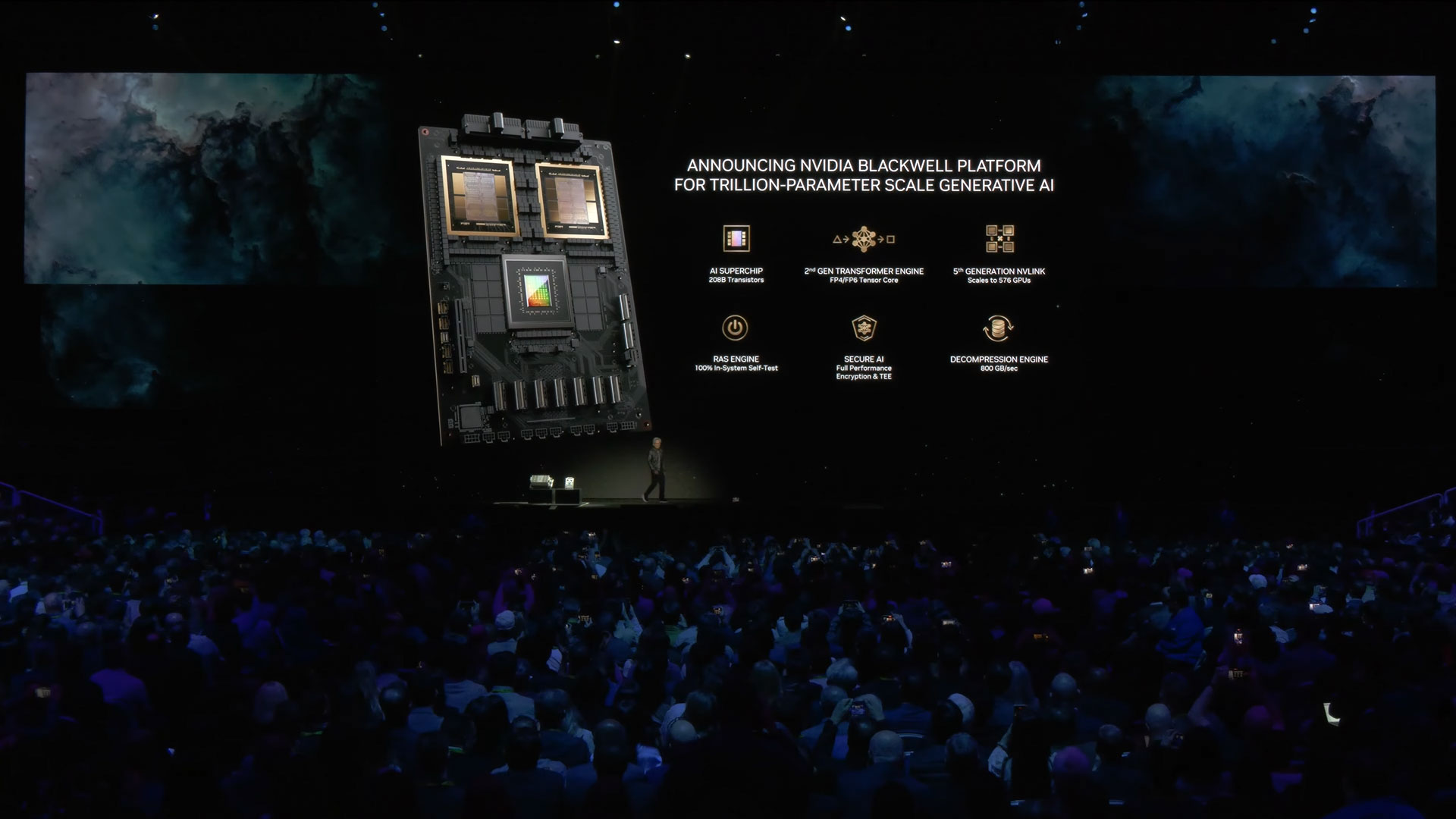
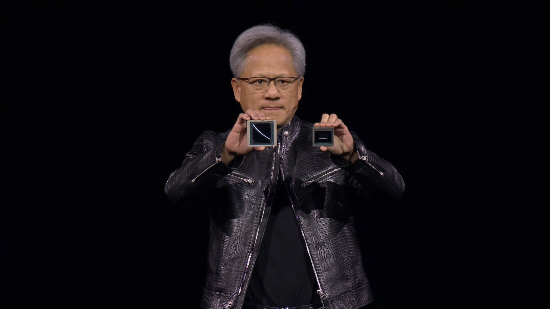
Nvidia currently sits atop the AI world, with data center GPUs that everybody wants. Its Hopper H100 and GH200 Grace Hopper superchip are in serious demand and power many of the most powerful supercomputers in the world. Well hang on to your seats: Nvidia just revealed the successor to Hopper. AT GTC 2024 today, CEO Jensen Huang dropped the Blackwell B200 bomb, the next-generation data center and AI GPU that will provide a massive generational leap in computational power.
The Blackwell architecture and B200 GPU take over from H100/H200. There will also be a Grace Blackwell GB200 superchip, which as you can guess by the name will keep the Grace CPU architecture but pair it with the updated Blackwell GPU. We anticipate Nvidia will eventually have consumer-class Blackwell GPUs as well, but those may not arrive until 2025 and will be quite different from the data center chips.
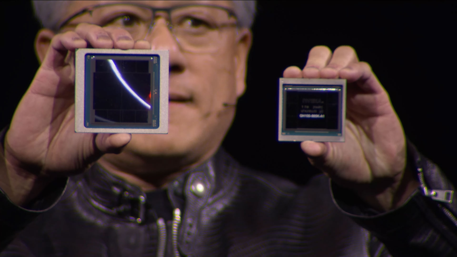
Nvidia Blackwell GPU
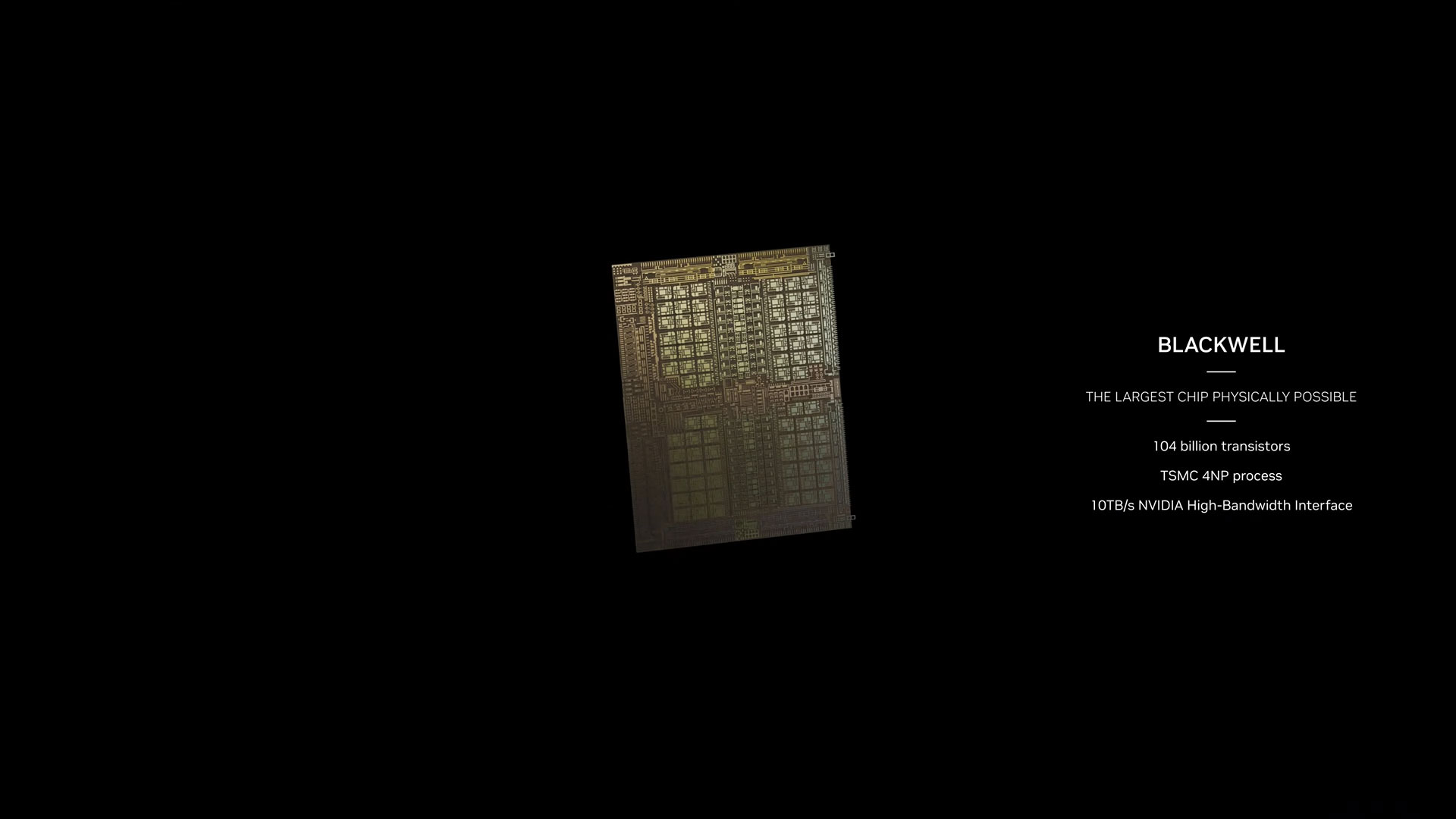
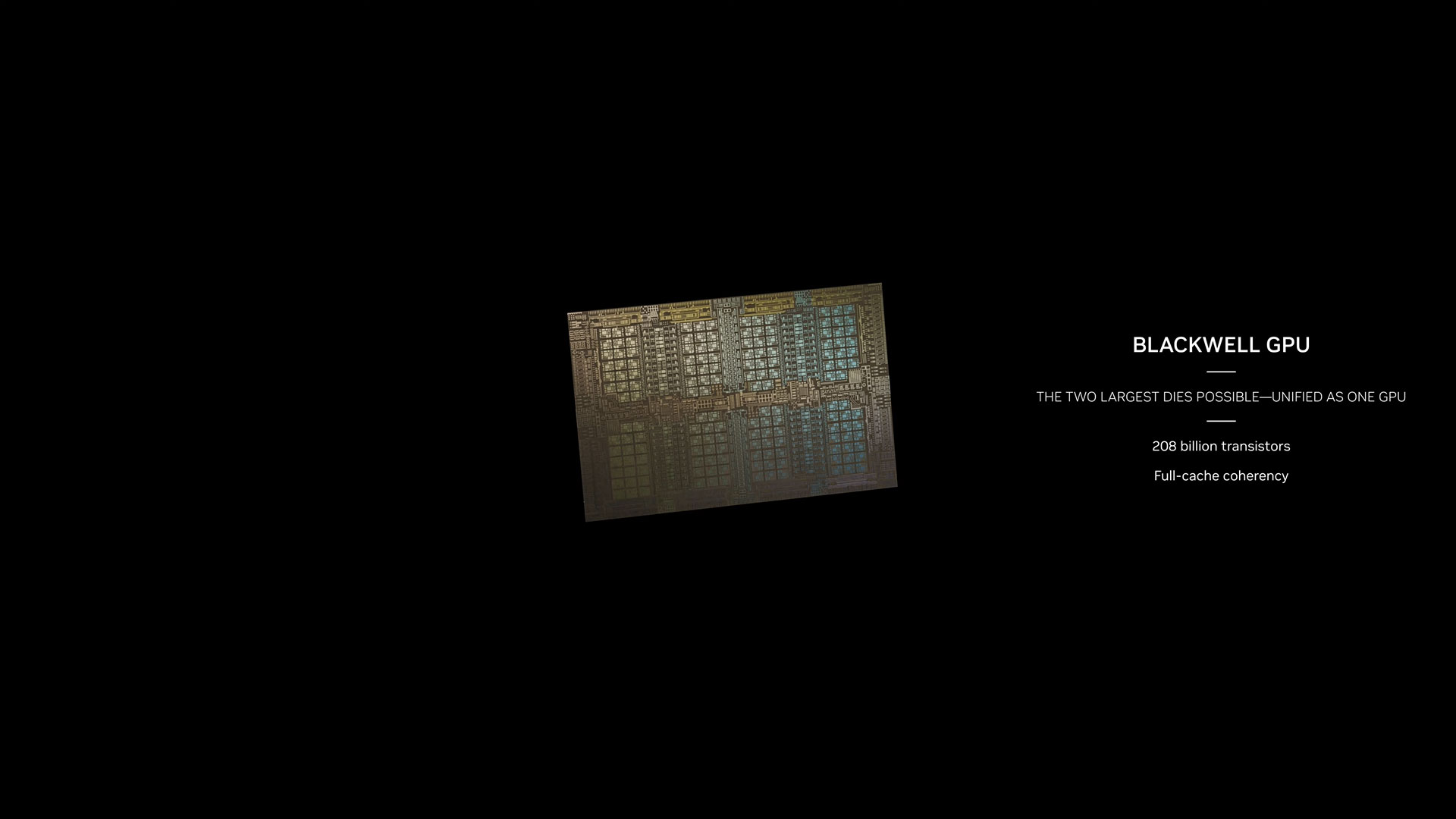
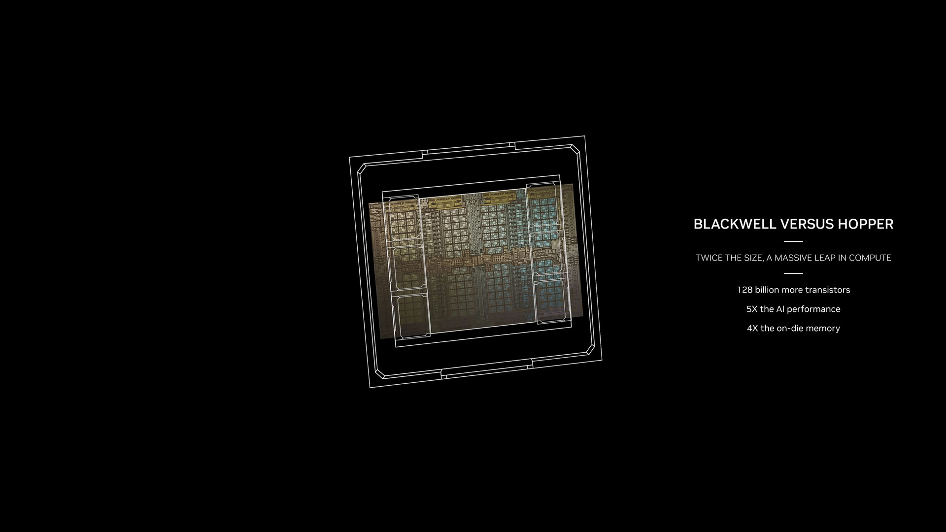
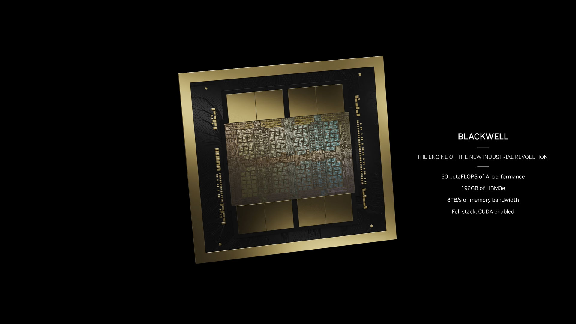
At a high level, the B200 GPU more than doubles the transistor count of the existing H100. There are some caveats that we’ll get to momentarily, but B200 packs 208 billion transistors (versus 80 billion on H100/H200). It also provides 20 petaflops of AI performance from a single GPU — a single H100 had a maximum 4 petaflops of AI compute. And last but not least, it will feature 192GB of HBM3e memory offering up 8 TB/s of bandwidth.
Now, let’s talk about some of the caveats. First and foremost, as the rumors have indicated, Blackwell B200 is not a single GPU in the traditional sense. Instead, it’s comprised of two tightly coupled die, though they do function as one unified CUDA GPU according to Nvidia. The two chips are linked via a 10 TB/s NV-HBI (Nvidia High Bandwidth Interface) connection to ensure they can properly function as a single fully coherent chip.
The reason for this dual-die configuration is simple: Blackwell B200 will use TSMC’s 4NP process node, a refined version of the 4N process used by the existing Hopper H100 and Ada Lovelace architecture GPUs. We don’t have a ton of details on TSMC 4NP, but it likely doesn’t offer a major improvement in feature density, which means if you want a more powerful chip, you need a way to go bigger. That’s difficult as H100 was basically already a full reticle size chip — it has a die size of 814 mm2, where the theoretical maximum is 858 mm2.
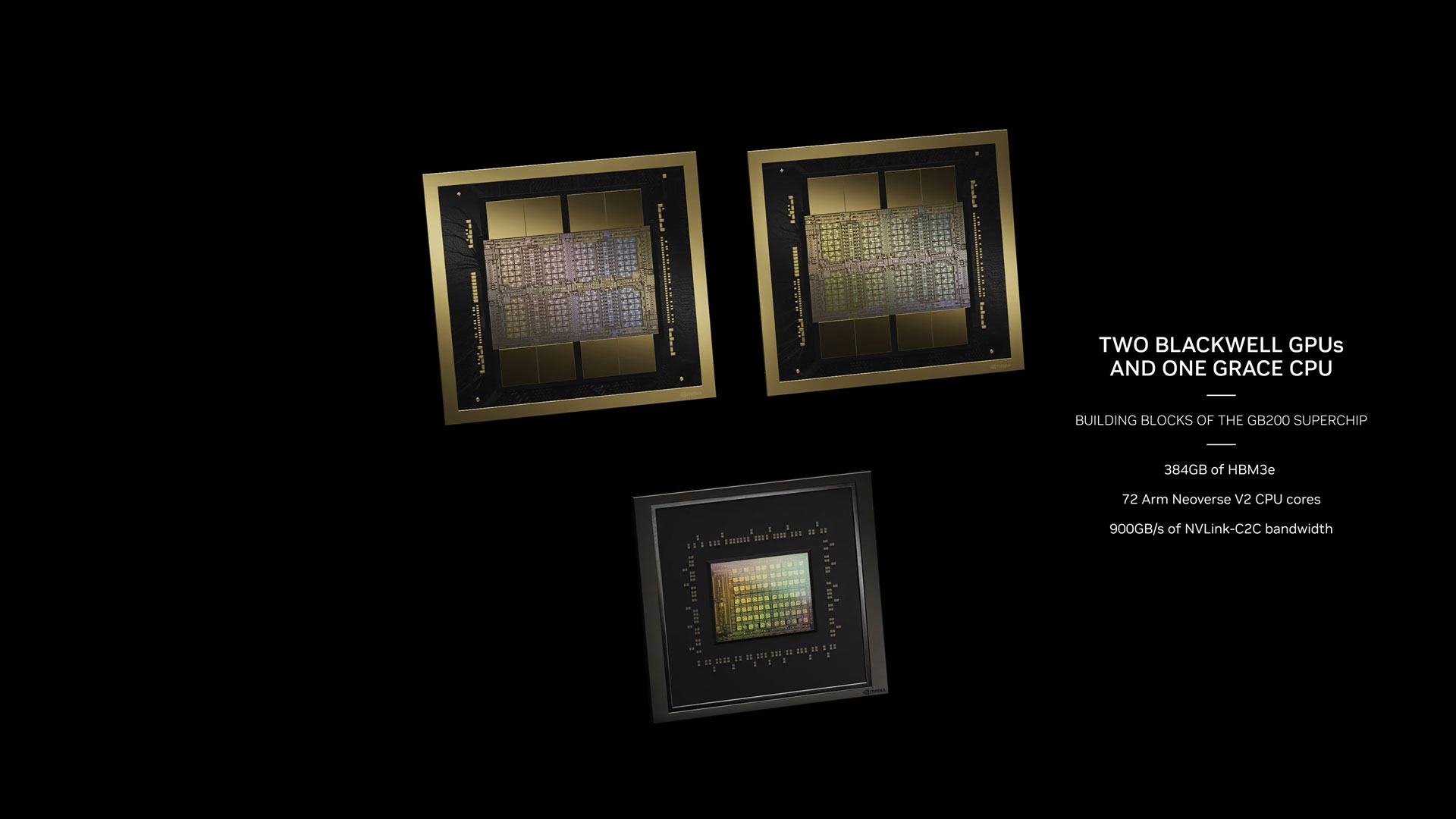
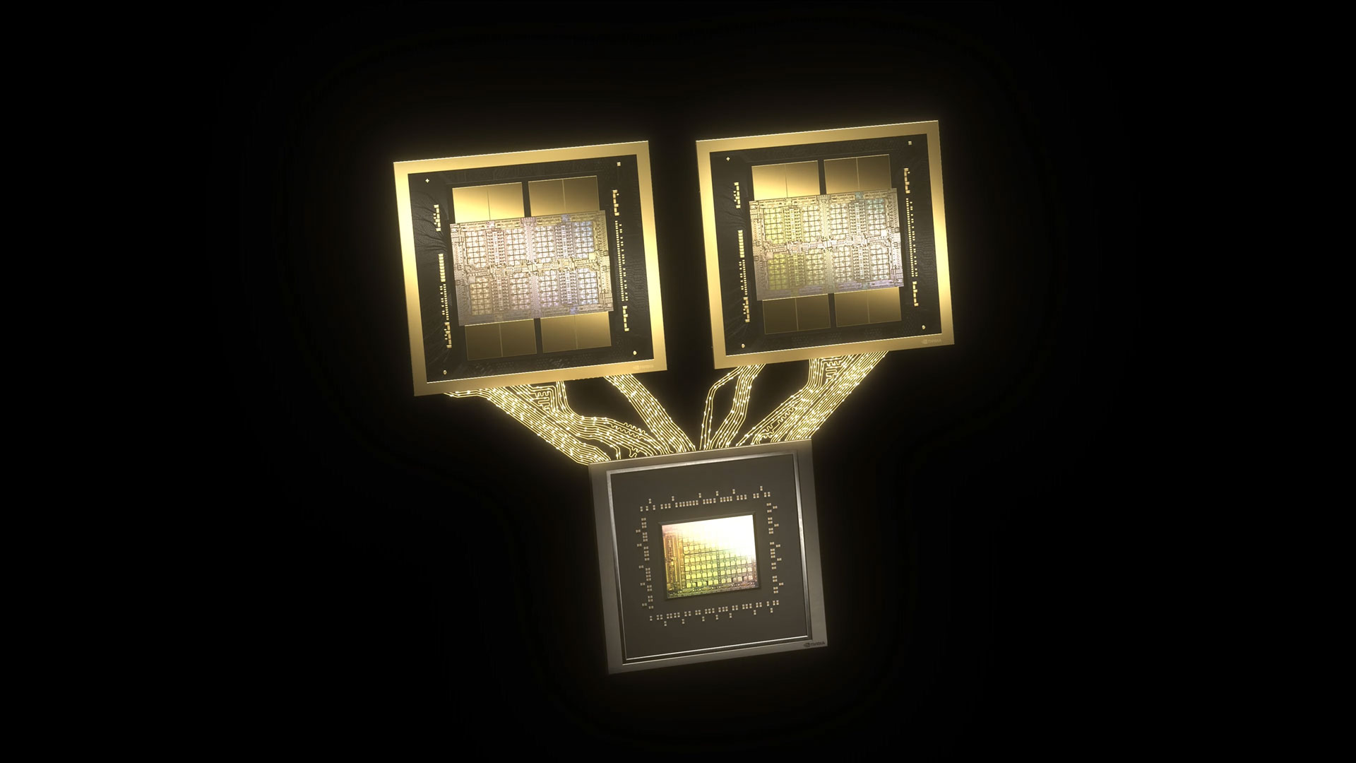
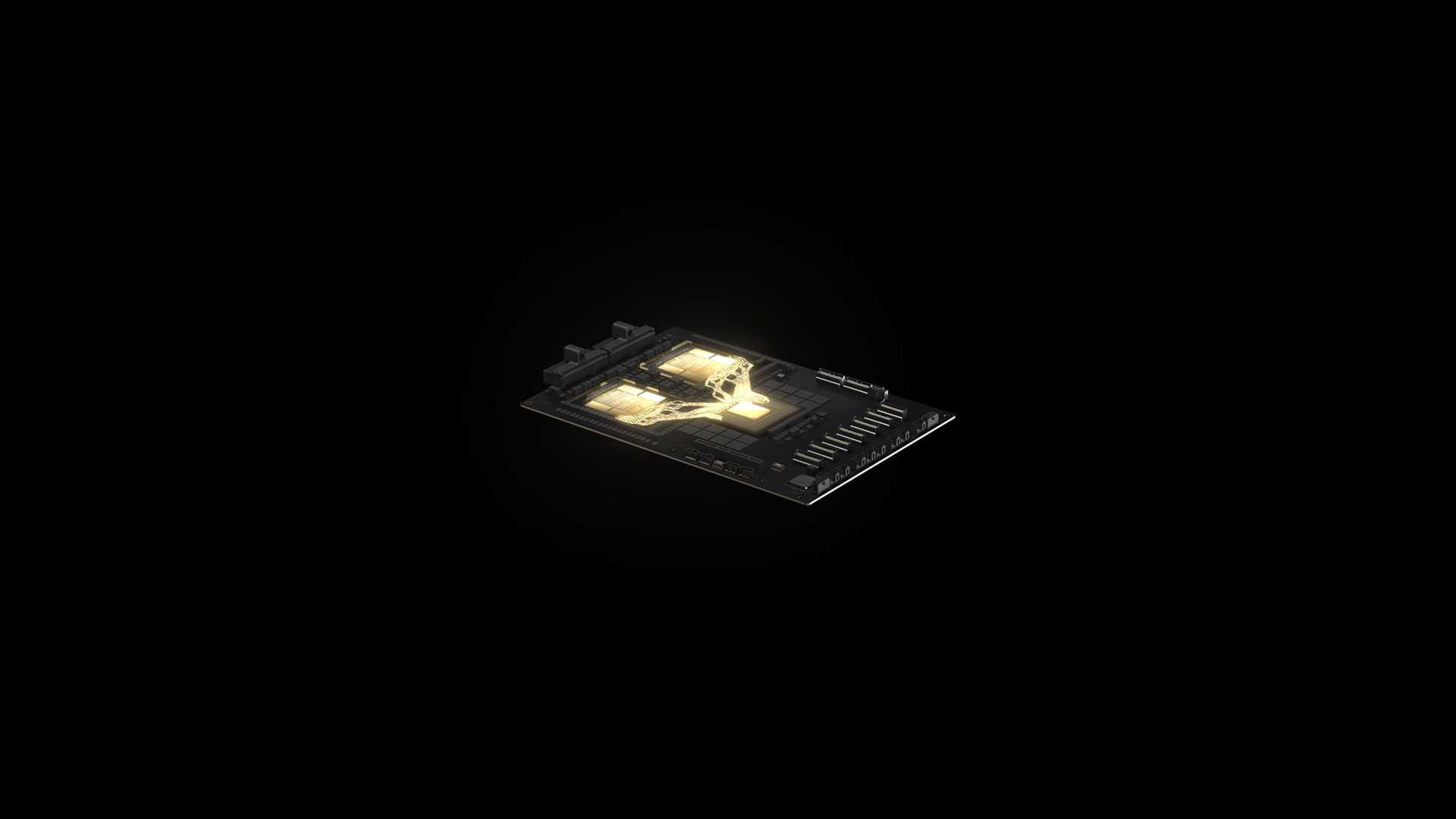
B200 will use two full reticle size chips, though Nvidia hasn’t provided an exact die size yet. Each die has four HMB3e stacks of 24GB each, with 1 TB/s of bandwidth each on a 1024-bit interface. Note that H100 had six HBM3 stacks of 16GB each (initially — H200 bumped this to six by 24GB), which means a decent chunk of the H100 die was dedicated to the six memory controllers. By dropping to four HBM interfaces per chip and linking two chips together, Nvidia can dedicate proportionately less die area to the memory interfaces.
The second caveat we need to discuss is with the maximum theoretical compute of 20 petaflops. Blackwell B200 gets to that figure via a new FP4 number format, with twice the throughput as Hopper H100’s FP8 format. So, if we were comparing apples to apples and sticking with FP8, B200 ‘only’ offers 2.5X more theoretical FP8 compute than H100 (with sparsity), and a big part of that comes from having two chips.
That’s an interesting point that again goes back to the lack of massive improvements in density from the 4NP process node. B200 ends up with theoretically 1.25X more compute per chip with most number formats that are supported by both H100 and B200. Removing two of the HBM3 interfaces and making a slightly larger chip might mean the compute density isn’t even significantly higher at the chip level — though of course the NV-HBI interface between the two chips also takes up some die area.
Nvidia provided the raw compute of other number formats with B200 as well, and the usual scaling factors apply. So the FP8 throughput is half the FP4 throughput at 10 petaflops, FP16/BF16 throughput is half again the FP8 figure at 5 petaflops, and TF32 support is half the FP16 rate at 2.5 petaflops — all of those with sparsity, so half those rates for dense operations. Again, that's 2.5X a single H100 in all cases.
What about FP64 throughput? H100 was rated at 60 teraflops of dense FP64 compute per GPU. If B200 had similar scaling to the other formats, each dual-die GPU would have 150 teraflops. However, it looks like Nvidia is stepping back FP64 performance a bit, with 45 teraflops of FP64 per GPU. But that also requires some clarification, as one of the key building blocks will be the GB200 superchip. That has two B200 GPUs and can do 90 teraflops of dense FP64, and other factors are at play that could improve the raw throughput on classical simulation compared to H100.
As far as utilizing FP4, Nvidia has a new second generation Transformer Engine that will help to automatically convert models to the appropriate format to reach maximum performance. Besides FP4 support, Blackwell will also support a new FP6 format, an in-between solution for situations where FP4 lacks the necessary precision but FP8 isn't needed either. Whatever the resulting precision, Nvidia classifies such use cases as "Mixture of Experts" (MoE) models.
We also need to clarify some things here, as there are multiple different variants of Blackwell available. Initially, Nvidia is providing specs in terms of full server nodes, and there are three main options. We've also broken out the two "single" GPUs based off the HGX configurations.
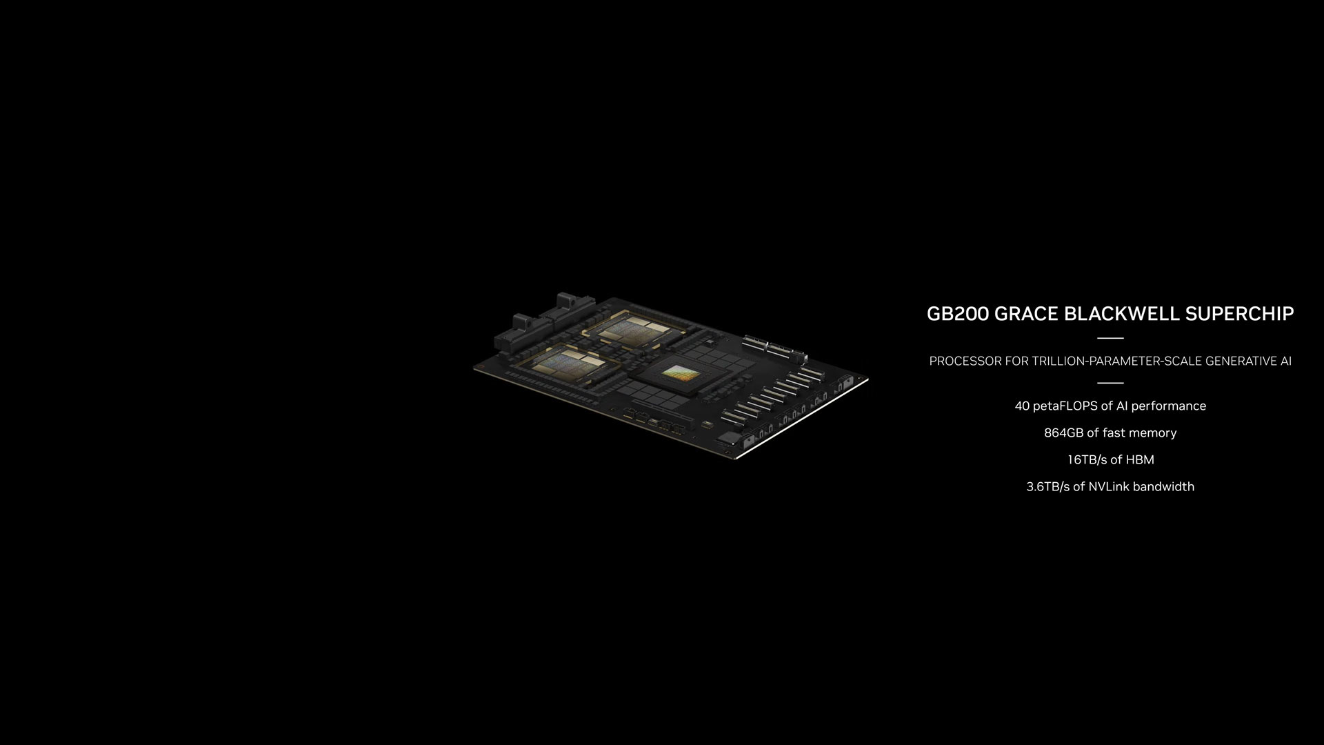
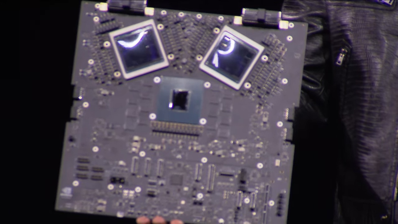
The largest and fastest solution will be a GB200 superchip, which we'll discuss more below, but as noted it has two B200 GPUs. The full superchip has a configurable TDP up to 2700W. That's for two GPUs (four GPU dies), plus a single Grace CPU. The numbers we just provided above — up to 20 petaflops of FP4 for a single B200 — are from half of a GB200 superchip. It's not clear what the TDP is for just a single B200 GPU in this configuration, but potentially it's up to 1400W for one GPUs, with both GPUs and the CPU sharing up to 2700W of combined power.
The next Blackwell option is the HGX B200, which is based on using eight B200 GPUs with an x86 CPU (probably two CPUs) in a single server node. These are configured with 1000W per B200 GPU, and the GPUs offer up to 18 petaflops of FP4 throughput — so on paper that's 10% slower than the GPUs in the GB200.
Finally, there will also be an HGX B100. It's the same basic idea as the HGX B200, with an x86 CPU and eight B100 GPUs, except it's designed to be drop-in compatible with existing HGX H100 infrastructure and allows for the most rapid deployment of Blackwell GPUs. As such, the TDP per GPU is limited to 700W, the same as the H100, and throughput drops to 14 petaflops of FP4 per GPU. There are likely other differences in the hardware that account for the B200 vs. B100 naming, besides the difference in TDP.
It's important to note that in all three of these servers, the HBM3e appears to be the same 8 TB/s of bandwidth per GPU. We would assume potential harvested dies for the lower tier parts, meaning fewer GPU cores and perhaps lower clocks, along with the difference in TDP. However, Nvidia has not revealed any details on how many CUDA cores or Streaming Multiprocessors will be available in any of the Blackwell GPUs yet.
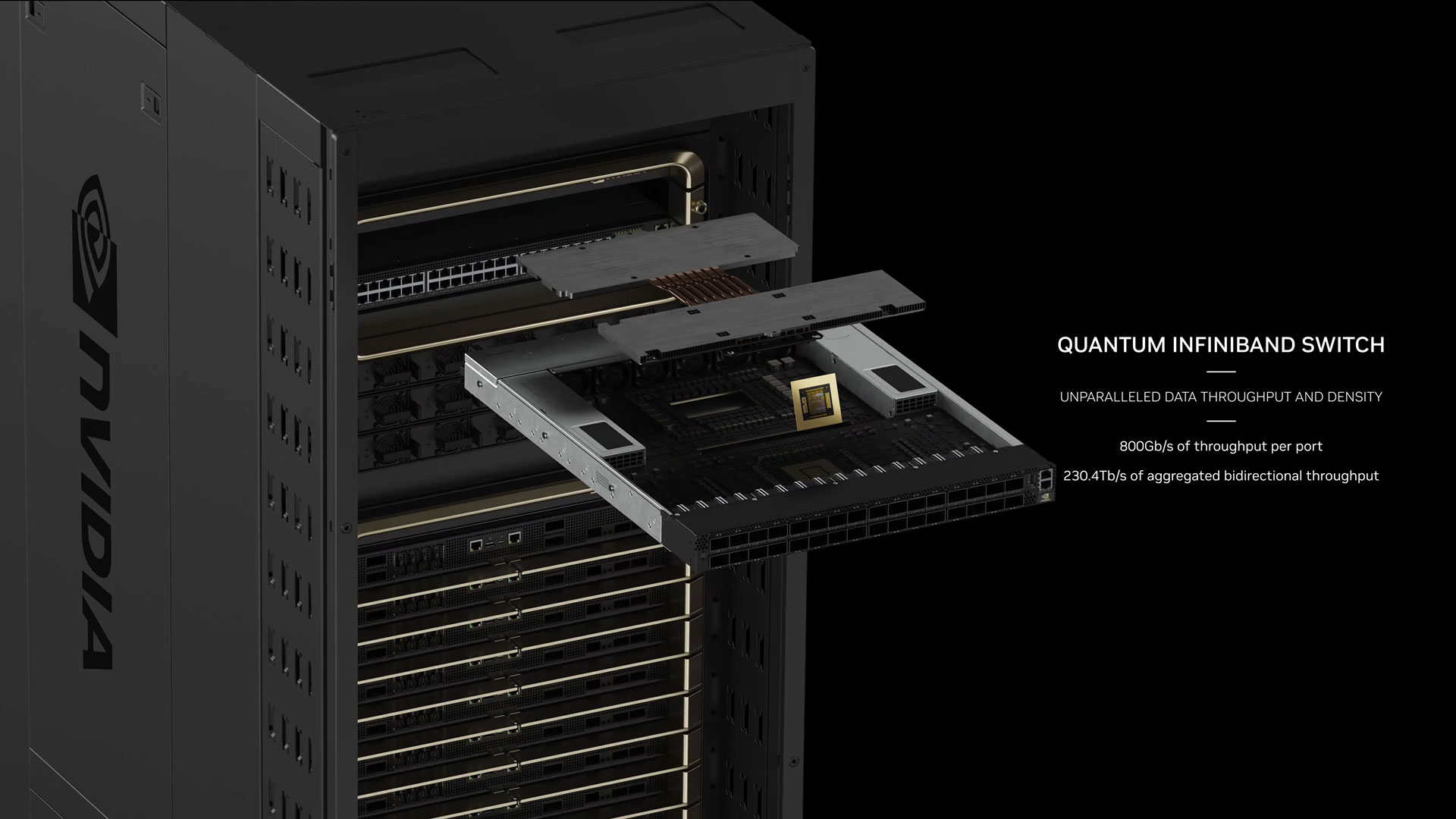
Nvidia NVLink 7.2T
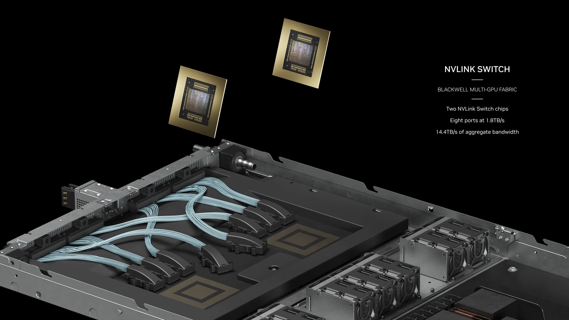
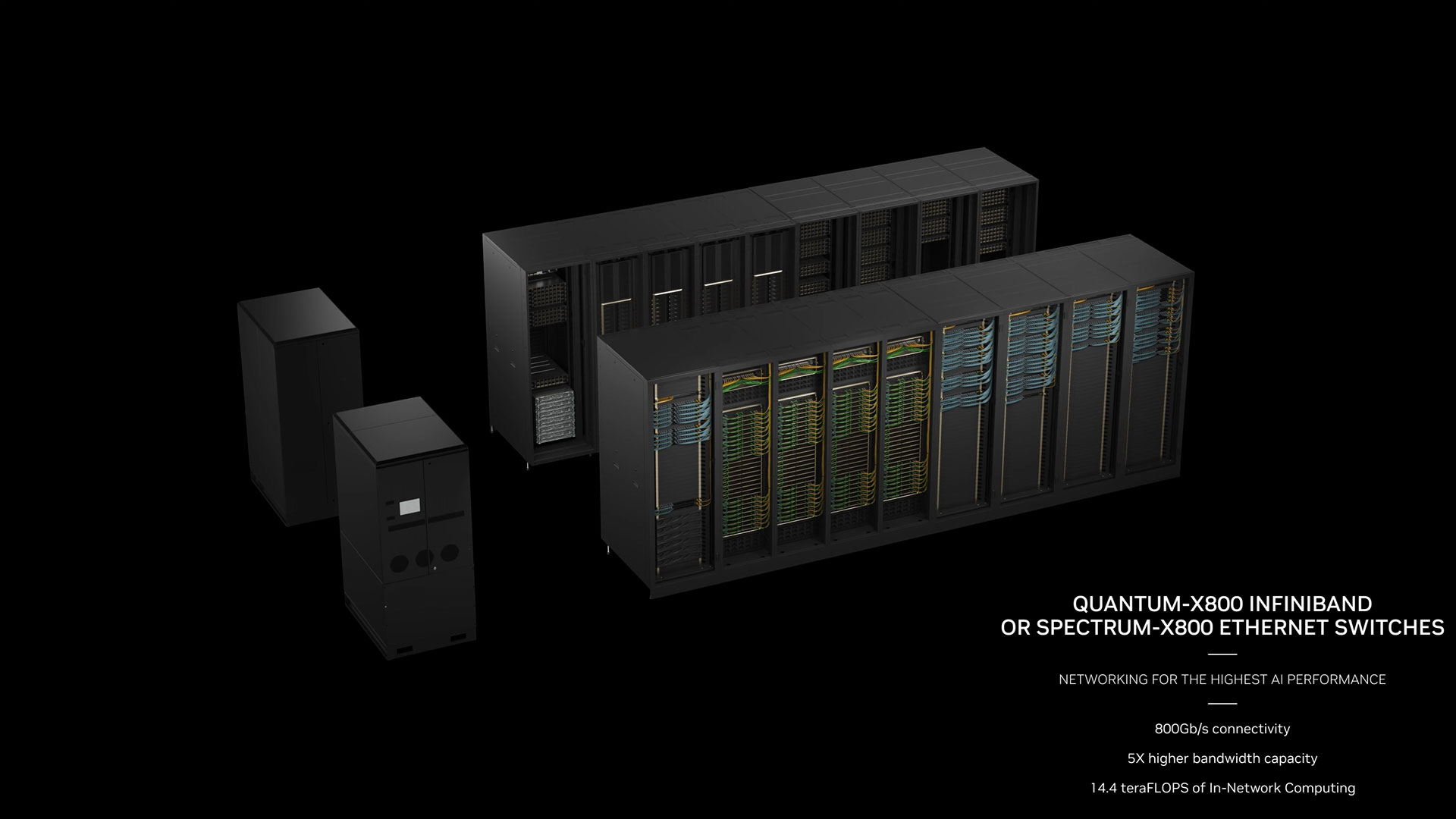
It’s not just about raw compute and memory bandwidth. One of the big limiting factors in AI and HPC workloads is the multi-node interconnect bandwidth for communication between different nodes. As the number of GPUs scales up, communication becomes a serious bottleneck and can account for up to 60% of the resources and time utilized. With B200, Nvidia is introducing its fifth generation NVLink and NVLink Switch 7.2T.
The new NVSwitch chip has 1.8 TB/s of all-to-all bidirectional bandwidth, with support for a 576 GPU NVLink domain. It’s a 50 billion transistor chip manufactured on the same TSMC 4NP node. That's relatively close to the size of Hopper H100 and shows how important the interconnect has become. The chip also supports 3.6 teraflops of Sharp v4 in-network compute on chip, which can help with the efficient processing of larger models — all that processing power can go toward intelligent load balancing of workloads.
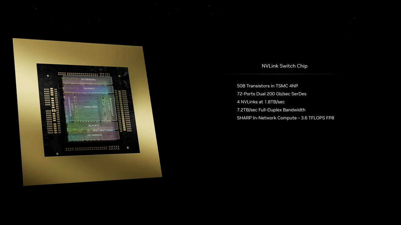
The previous generation supported up to 100 GB/s of HDR InfiniBand bandwidth, so this is a huge jump in bandwidth. The new NVSwitch offers an 18X speedup compared to the H100 multi-node interconnect. This should enable significantly improved scaling for larger trillion parameter model AI networks.
Related to this, each Blackwell GPU comes equipped with 18 fifth generation NVLink connections. That's eighteen times as many links as H100. Each link offers 50 GB/s of bidirectional bandwidth, or 100 GB/s per link, which will help tremendously when scaling to larger models. In a sense, it allows larger groups of GPU nodes to function on some levels as though they're just a single massive GPU.
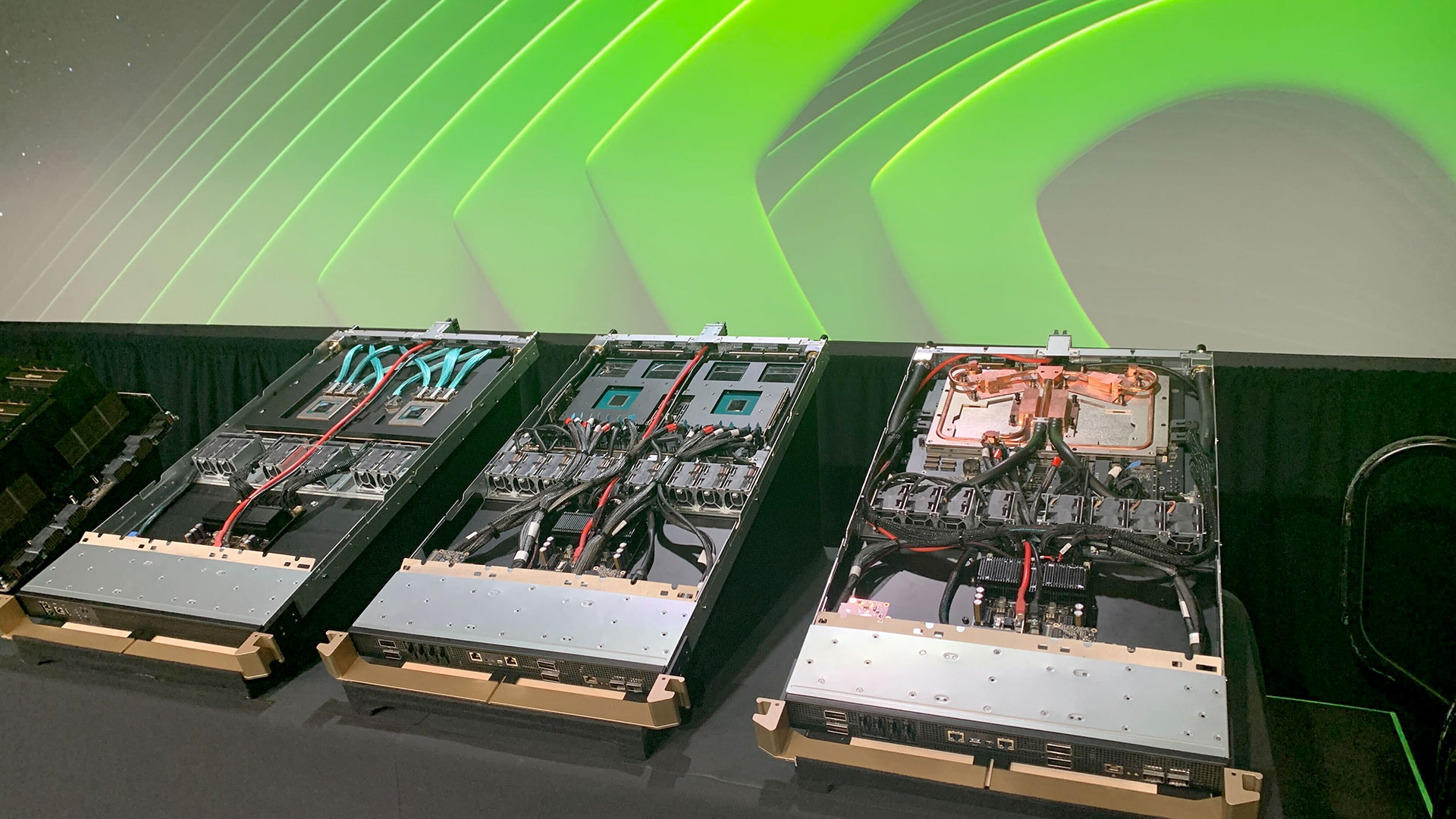
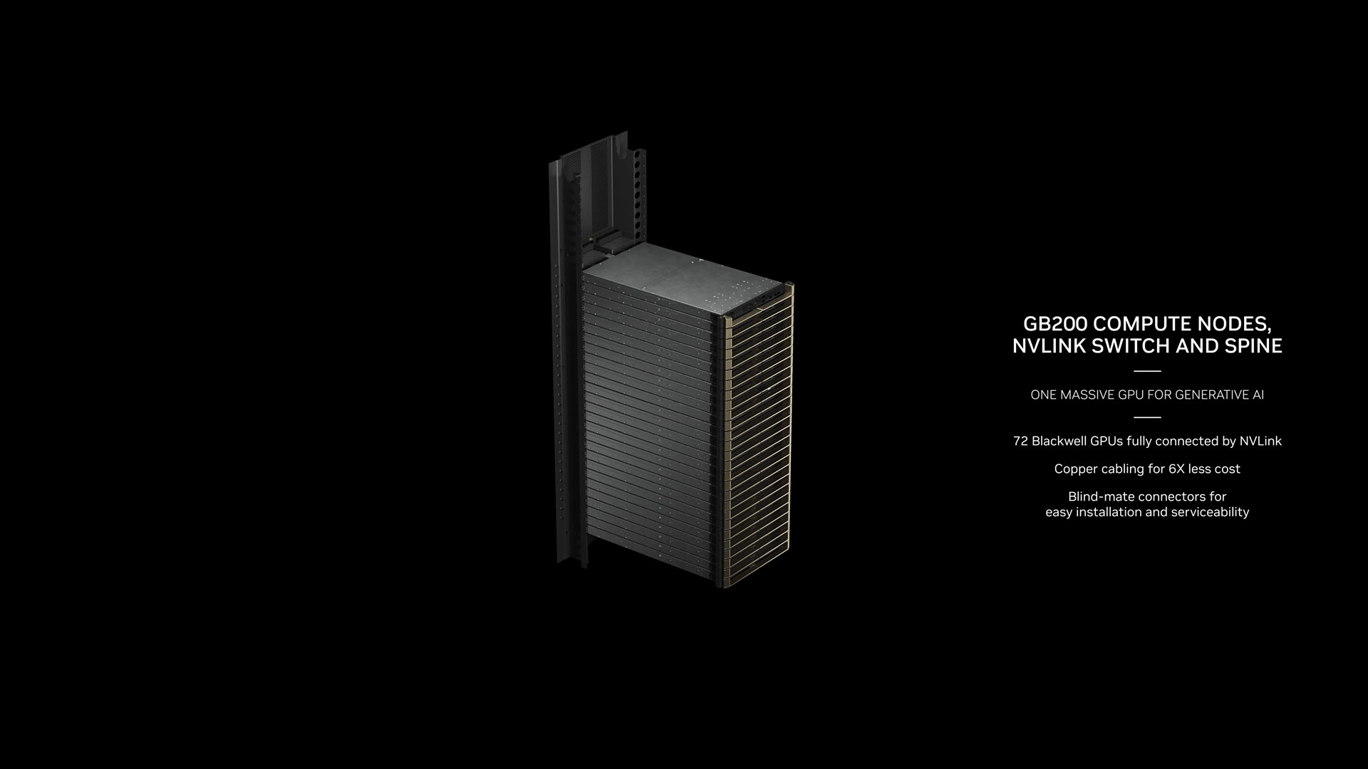
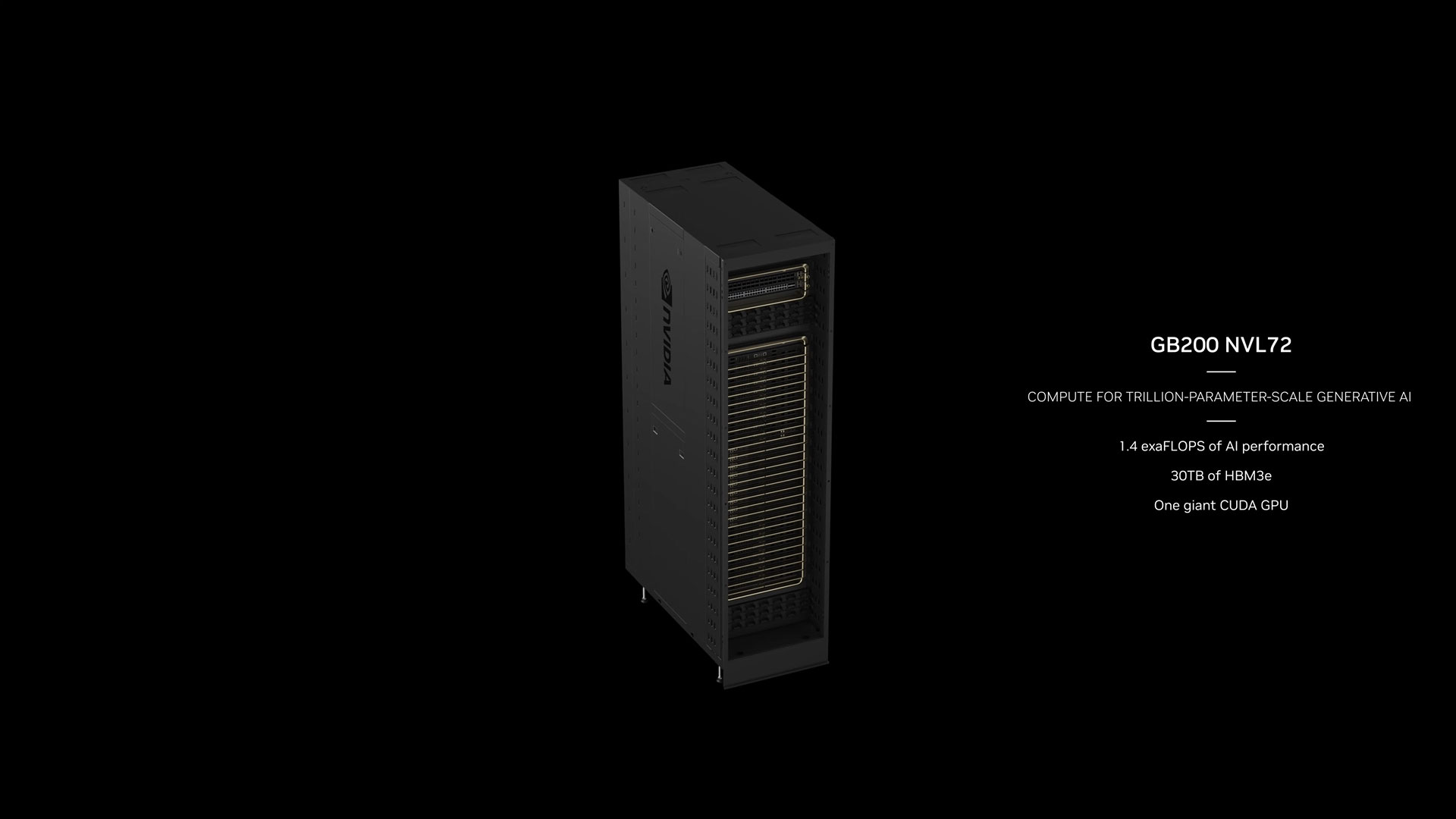
Nvidia B200 NVL72
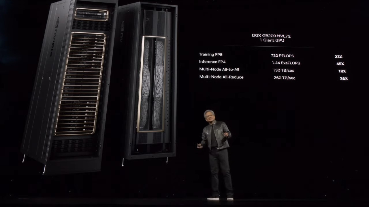
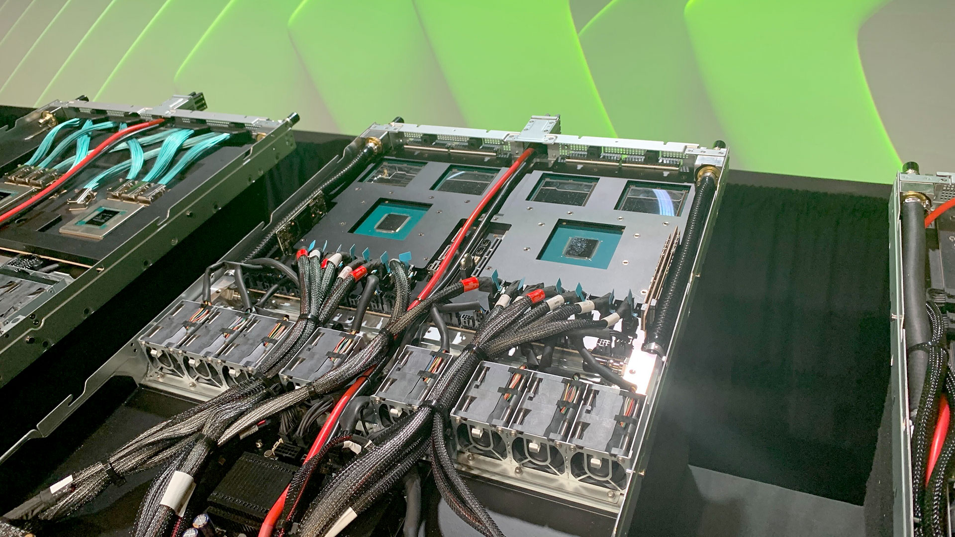
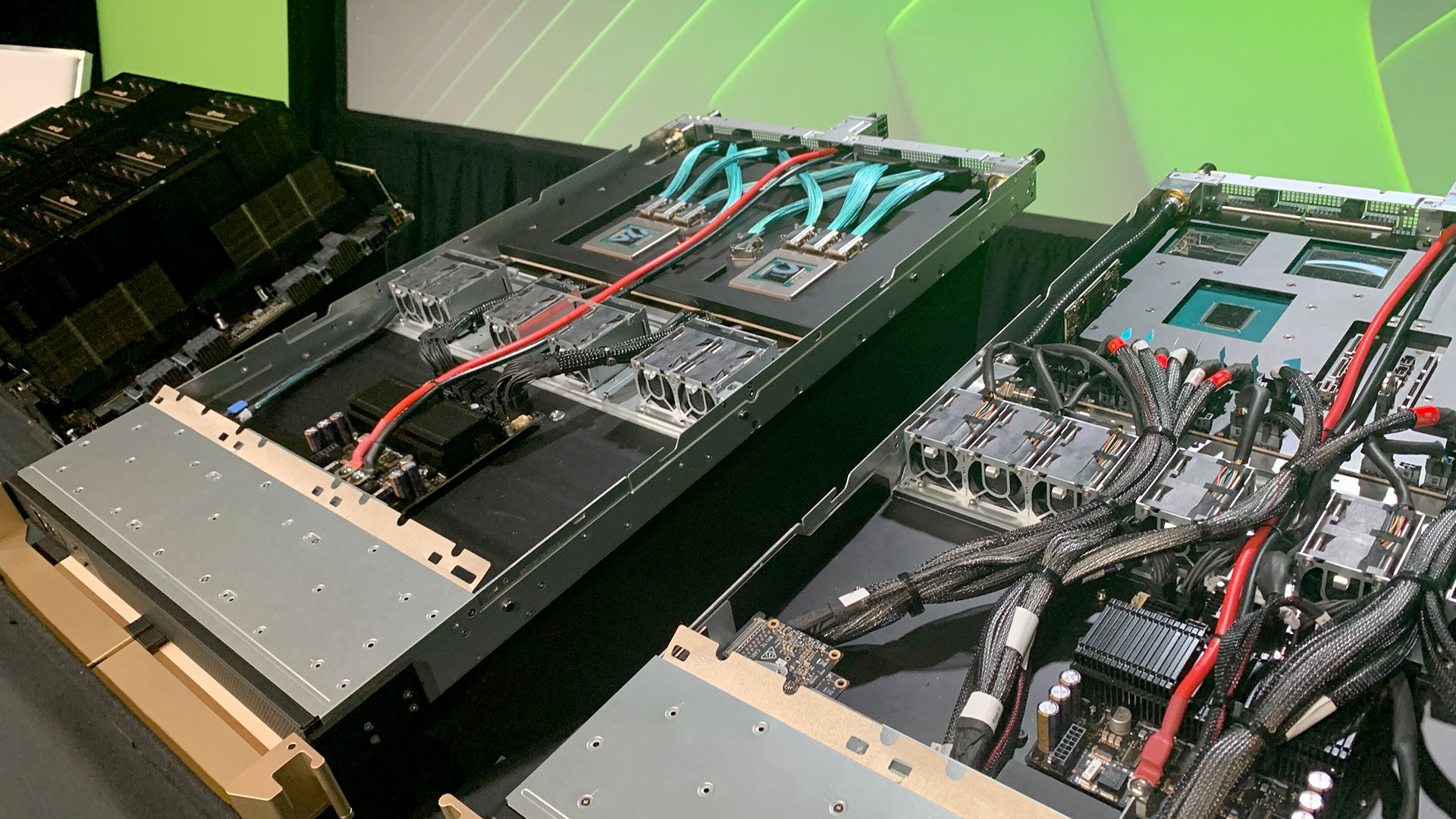
Take the above and put them together and you get Nvidia’s new GB200 NVL72 systems. These are basically a full rack solution, with 18 1U servers that each have two GB200 superchips. There are some differences compared to the prior generation here, however, in terms of what constitutes a GB200 superchip. There are two B200 GPUs paired with a single Grace CPU, whereas GH100 used a smaller solution that put a single Grace CPU alongside a single H100 GPU.
Each compute node in the GB200 NVL72 has two GB200 superchips, so a single compute tray has two Grace CPUs and four B200 GPUs, with 80 petaflops of FP4 AI inference and 40 petaflops of FP8 AI training performance. These are liquid-cooled 1U servers, and they take up a large portion of the typical 42 units of space offered in a rack.
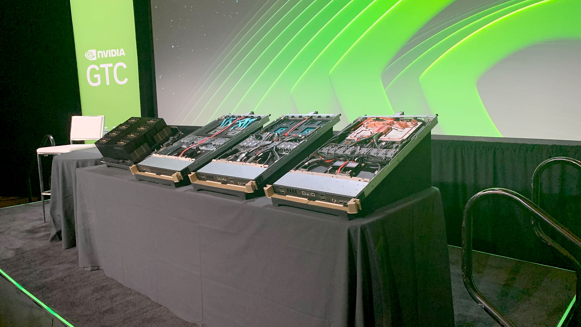
Alongside the GB200 superchip compute trays, the GB200 NVL72 will also feature NVLink switch trays. These are also 1U liquid-cooled trays, with two NVLink switches per tray, and nine of these trays per rack. Each tray offers 14.4 TB/s of total bandwidth, plus the aforementioned Sharp v4 compute.
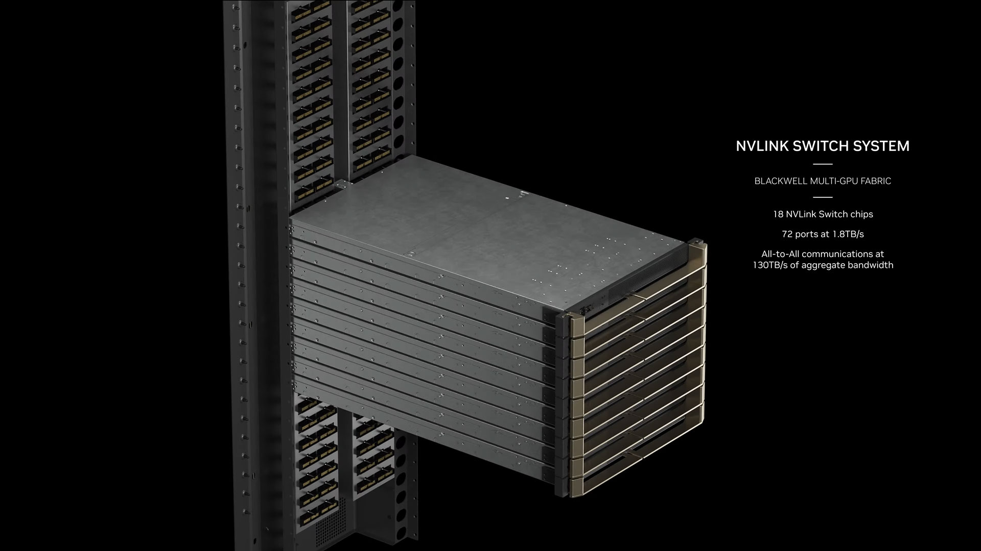
Altogether, the GB200 NVL72 has 36 Grace CPUs and 72 Blackwell GPUs, with 720 petaflops of FP8 and 1,440 petaflops of FP4 compute. There’s 130 TB/s of multi-node bandwidth, and Nvidia says the NVL72 can handle up to 27 trillion parameter models for AI LLMs. The remaining rack units are for networking and other data center elements.
Nvidia B200 SuperPOD
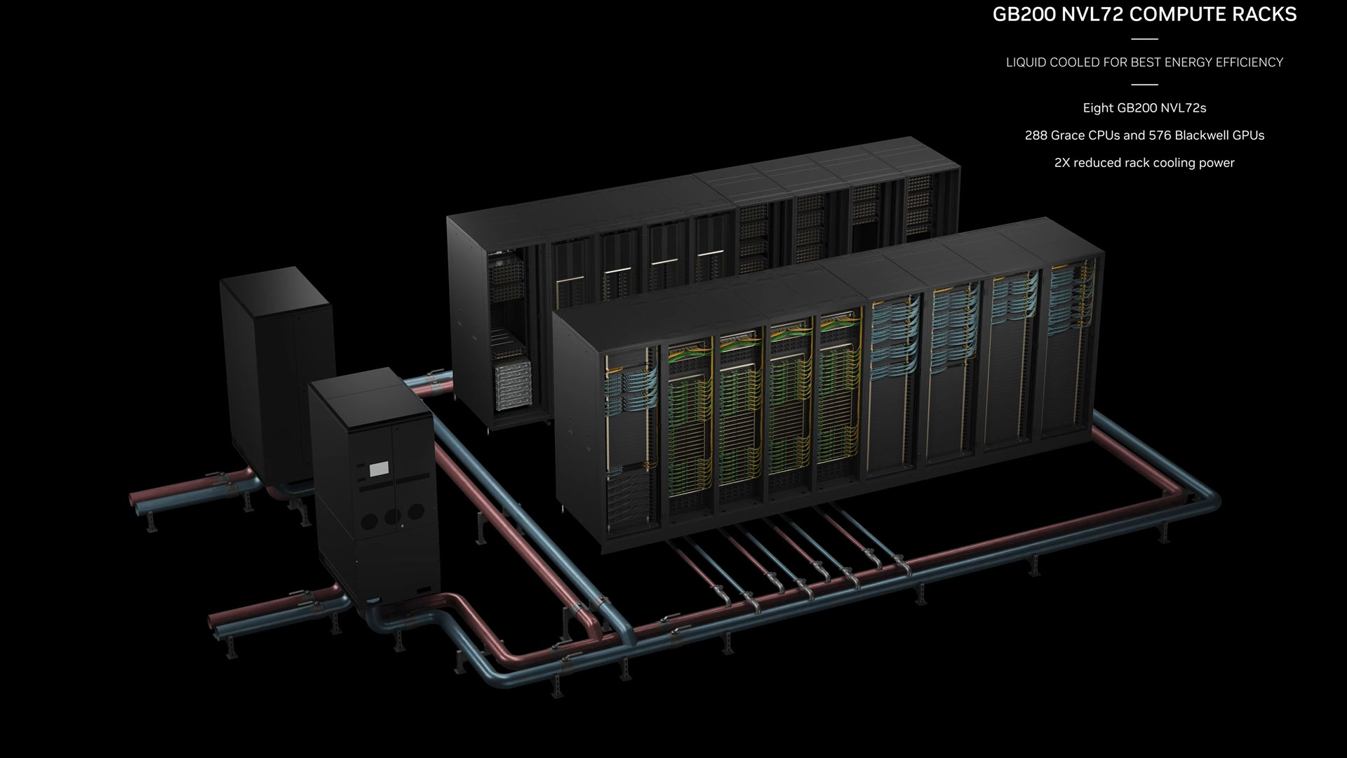
Wrapping things up, we have the new SuperPODs with GB200 systems. We noted earlier that the latest NVLink chips support up to a 576 GPU domain. That’s important, because the new DGX SuperPOD scales to precisely that number of GB200 Blackwell GPUs. Each SuperPOD can house up to eight GB200 NVL72 systems, which works out to 288 Grace CPUs and 576 B200 GPUs.
The full SuperPOD is quite the AI supercomputer in itself, with 240TB of fast memory and 11.5 exaflops of FP4 compute — or if you prefer, 5.75 exaflops of FP8 or 2.88 exaflops of FP16. Installations can scale to many SuperPODs, with potentially tens of thousands of Blackwell GPUs and Grace CPUs.
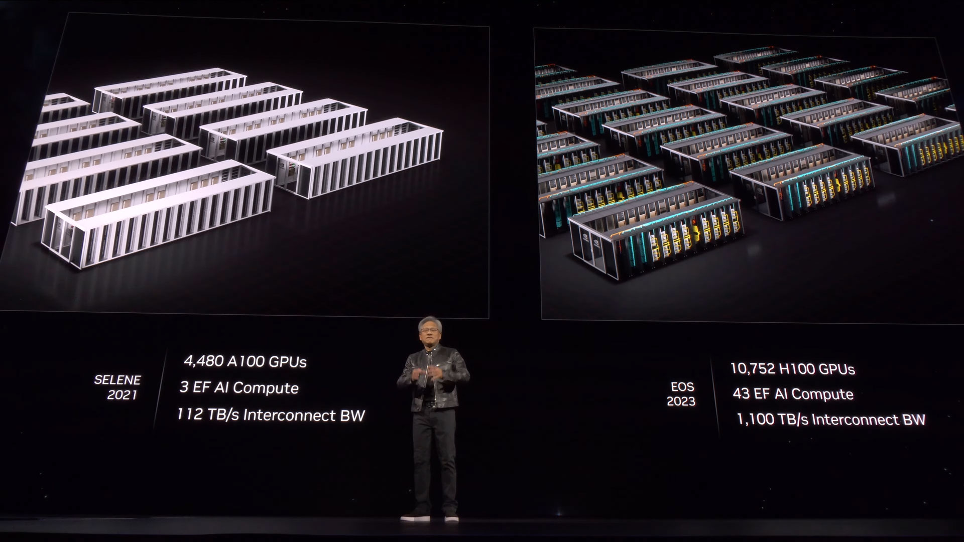
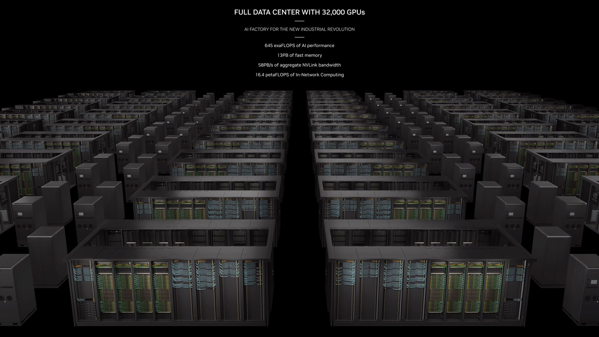
While nothing was said, we're guessing Nvidia is already starting or will soon begin installing GB200 SuperPODs in either a new supercomputer, or perhaps as an expansion of its existing Eos supercomputer. Nvidia did provide an example installation with a hypothetical 56 SuperPODs and over 32,000 total B200 GPUs. Should that become a reality, it would be an AI supercomputer with 645 exaflops of FP4 compute, 13PB of HBM3e memory, , 58 PB/s of aggregate NVLink bandwidth, and 16.4 petaflops of in-network compute.
The SuperPODs are intended to scale up to trillion parameter AI datasets, and Nvidia says compared to H100 solutions, each SuperPOD offers a 4X increase in training performance, and up to a 30X increase in inference speeds. It also claims up to a 25X improvement in energy efficiency compared to the previous H100 based solutions, though the comparison is clearly not something that will apply universally. In this case, it's using the same number of GPUs, running a "massive model" and using the new FP4 number format.
Nvidia will also offer DGX B200 systems, which will presumably use Xeon or EPYC processors instead of Grace. These systems are for workloads that specifically want x86 support. Nvidia says DGX B200 can deliver up to a 3X increase in training speed, 15X for inference, and 12X energy savings.
As with the previous A100 and H100 SuperPODs, these are designed to offer a quick scale-up solution for data centers and cloud service providers. Nvidia is working with Amazon Web Services, Google Cloud, and Oracle Cloud to offer GB200 NVL72 solutions, and says that AWS will have Project Ceiba that will have over 20,000 B200 GPUs, 4PB of HBM3e memory, and over 400 exaflops of AI compute in the coming months.
The Blackwell Tour de Force
Nvidia is throwing down the gauntlet again with Blackwell and its related technologies. The company was already at the top of the AI heap, and it knows where the biggest bottlenecks lie and how to address them. From the core GPU to the interlinks to the node-to-node communications, the Blackwell ecosystem looks to shore up any potential shortcomings of the previous solutions.
The previous Hopper H100 and Ampere A100 solutions have proven incredibly prescient and successful for Nvidia. Whoever is looking in a crystal ball trying to predict where the industry is heading next nailed it with these AI solutions. CEO Jensen recently quipped that Nvidia's competitors couldn't give their AI solutions away — shots fired back at those claiming Nvidia's dominance was "pure luck", no doubt. Whatever the cause, the result is that Nvidia's latest earnings show an obscene 126% year-over-year increase, with over a 600% improvement for the latest quarter compared to one year ago in the data center division.
It's a safe bet that things aren't going to slow down any time soon with Blackwell. Nvidia has more than doubled down on the GPU size, with dual chips and major overhauls to the underlying hardware. The Grace Blackwell GB200 superchip also represents another doubling down, with two full B200 GPUs paired to a single Grace CPU for the "superchip" module. Blackwell is also designed to scale to much larger installations than Hopper, enabling ever larger AI models.
How much will Blackwell solutions cost compared to Hopper? Nvidia didn't say, but with H100 GPUs generally going for around $40,000 each, and given everything that's involved with Blackwell, $100,000 per GPU wouldn't be surprising.
The competition isn't standing still, obviously, and just about every major tech company is talking about AI and deep learning and how they're going to be at the forefront of the AI revolution. But talk is cheap, and Nvidia is already at the head of the pack. It invested big into AI starting about a decade back and is now reaping the fruits of those investments, and at least for the next year or two, Blackwell looks like it will power the most advanced AI installations.
Blackwell B200 hardware should begin full production and shipping later in 2024. Nvidia hasn't committed to an exact timeframe yet, but additional details will be revealed in the coming months.