
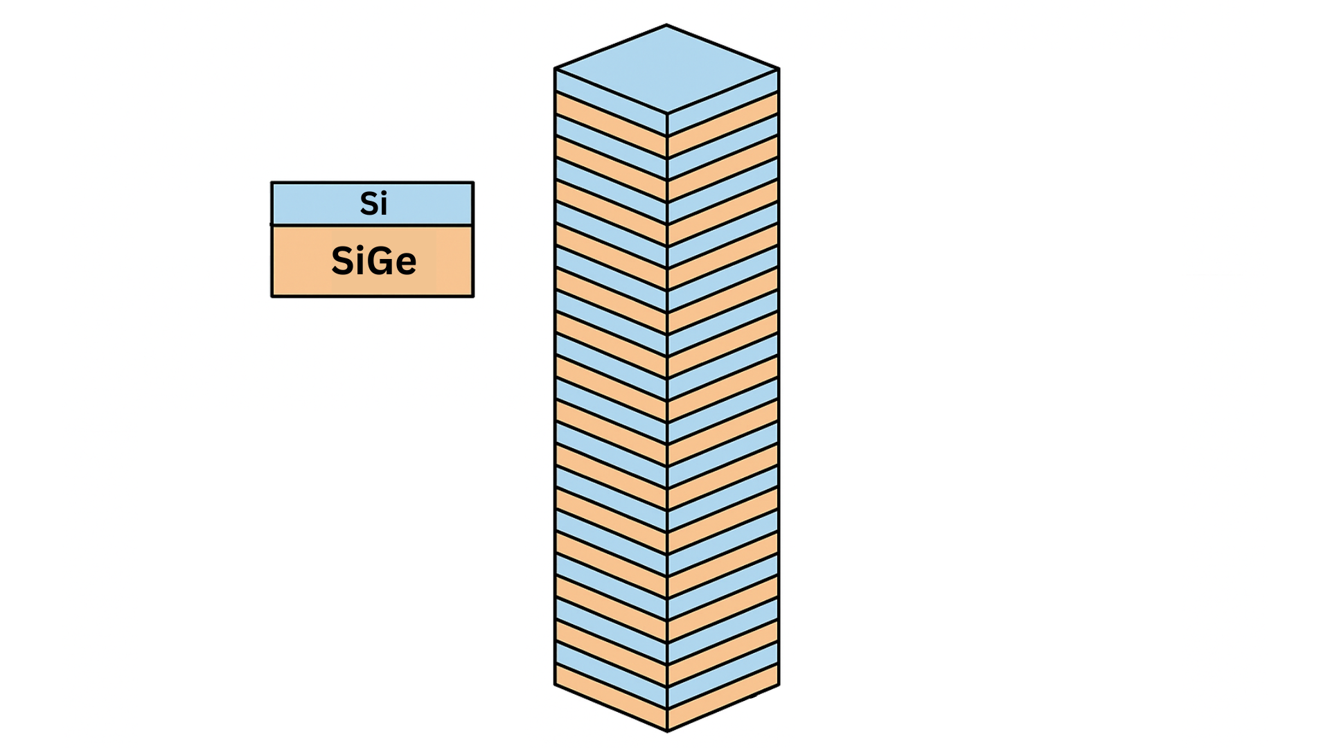
Imagine trying to build a tower out of hundreds of very thin, slightly different sheets of material, where each sheet wants to bend or warp on its own. That’s essentially what researchers at imec and Ghent University accomplished when they grew 120 alternating layers of silicon (Si) and silicon-germanium (SiGe) on a 300 mm wafer—a key step toward three-dimensional DRAM. At first glance, it sounds like stacking sheets of paper; in reality, it’s more like balancing a house of cards with materials that naturally want to pull apart.
The challenge starts with lattice mismatch. Silicon and silicon-germanium crystals have slightly different atomic spacings, so when stacked, the layers naturally want to stretch or compress. Think of it like trying to stack a deck of cards where every second card is slightly larger than the first—without careful alignment, the stack warps and topples. In semiconductor terms, these “topples” appear as misfit dislocations, tiny defects that can ruin a memory chip’s performance.
To solve this, the team carefully tuned the germanium content in the SiGe layers and experimented with adding carbon, which acts like a subtle glue that relieves stress. They also maintained extremely uniform temperatures during the deposition process, because even minor hot or cold spots in the reactor can lead to uneven growth.
The process itself, using advanced epitaxial deposition techniques, is like painting with gases. Silane and germane—gases containing silicon and germanium—are broken down on the wafer surface, leaving behind precise, nanometer-thin layers. Controlling the thickness, composition, and uniformity of each layer is crucial; even a tiny deviation can propagate through the stack, magnifying defects.
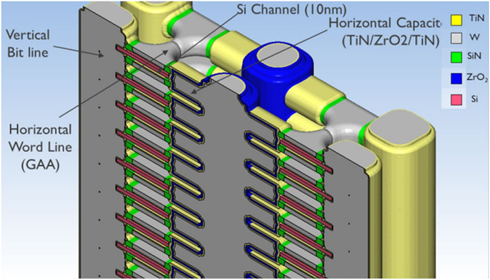
Now, why go through all this effort? In conventional DRAM, memory cells are laid out flat, limiting density. Stacking layers vertically—in 3D—allows for far more memory cells in the same footprint, improving storage capacity without making chips larger. Successfully creating 120 bilayers demonstrates that vertical scaling is achievable, bringing us closer to next-generation, high-density memory devices.
Think of each bilayer as a story in a skyscraper, if one floor is misaligned then the entire building becomes unstable. By controlling strain and keeping layers uniform, the researchers effectively built a nanoscale skyscraper of silicon and SiGe that could host thousands of memory cells per unit area.
The implications stretch beyond memory chips. Techniques for growing precise multi-layer structures can advance 3D transistors, stacked logic devices, and even quantum computing architectures, where controlling layer properties at the atomic level is critical. Samsung has already put 3D DRAM on its roadmap and even has a dedicated R&D facility for it.
Want more? We've got an exclusive roadmap to the future of 3D NAND flash — only for subscribers of Tom's Hardware Premium.
Furthermore, the research aligns with ongoing efforts to develop Gate-All-Around Field-Effect Transistor (GAAFET) and Complementary FET (CFET) technologies. These advanced transistor architectures benefit from the precise control over material properties afforded by epitaxial growth techniques, enabling the fabrication of smaller, more powerful transistors that are crucial for the continued miniaturization of electronic devices.
In summary, this is not just stacking silicon as you might know; it’s engineering order from atomic tension, creating structures that nature itself would struggle to produce. For memory technology, like we say with every new breakthrough, it’s a milestone that could reshape how chips are designed, making them denser, faster, and more reliable than ever before.
Follow Tom's Hardware on Google News to get our up-to-date news, analysis, and reviews in your feeds. Make sure to click the Follow button.