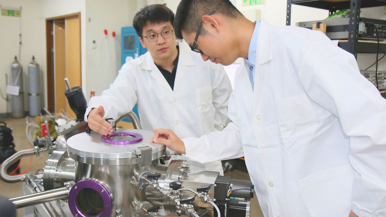
A cross-institutional research team has published a paper where a breakthrough in (MRAM) development is detailed. According to a blog post published by Taiwan’s National Yang Ming Chiao Tung University (NYCU), which spearheaded the efforts, they have managed to overcome a major challenge that hampered the development and adoption of this kind of non-volatile memory. The researchers claim that their spin–orbit torque magnetic random-access memory (SOT-MRAM) is a true next-gen breakthrough as it offers ~1ns switching speeds, and data retention exceeding 10 years, among its multitude of attractions.
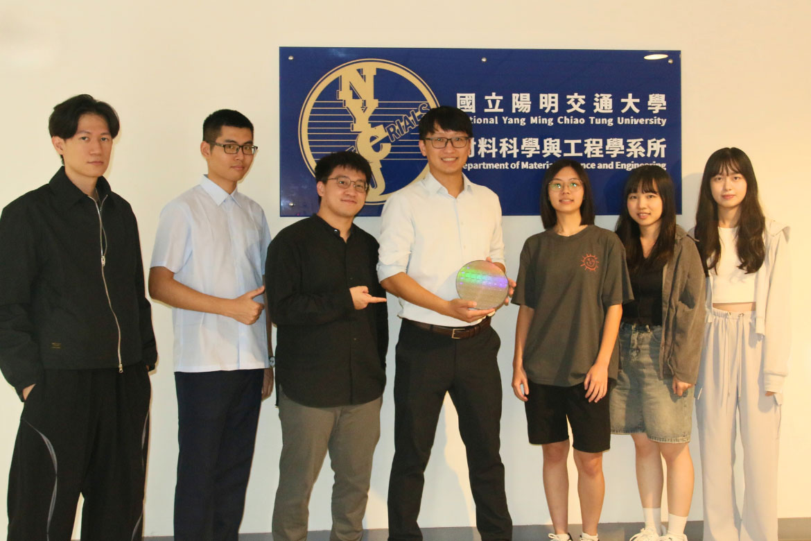
This latest SOT-MRAM development comes from a cross-institutional collaboration between Taiwan’s National Yang Ming Chiao Tung University (NYCU), leading chip foundry TSMC, Taiwan’s Industrial Technology Research Institute (ITRI), the National Synchrotron Radiation Research Center (NSRRC) in Taiwan, Stanford University, and National Chung Hsing University (NCHU) in Taiwan. We’ve covered the same team’s earlier advances in building a SOT-MRAM array chip (Jan 2024) but much progress has been made since then.
Tungsten layer
The key advance presented in the recently published paper is the introduction of a tungsten layer to generate the spin currents. Specifically, the team managed to stabilize the rare beta-phase of Tungsten, which is crucial for increased performance – and will be even more important for eventual mass production of SOT-MRAM devices.
Last year, we noted that NYCU’s SOT-MRAM was capable of latencies up to 10ns. Now it has been improved to ~1ns, rivaling SRAM, reveals testing of a 64kb array the scientists built. For further context, that is slightly faster than DRAM (DDR5 has latency around 14ms) and considerably faster than 3D TLC NAND (which has read latencies between 50 and 100 microseconds).
Don’t forget, though, that this new SOT-MRAM brings the benefits of non-volatility. Other trumpeted advances delivered by the latest SOT-MRAM device demo were:
- Ultrafast switching speeds (as fast as one nanosecond)
- Data retention exceeding 10 years
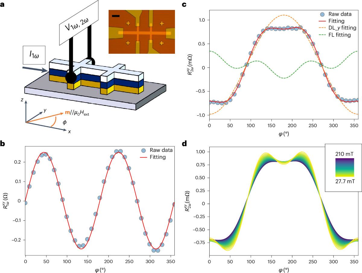
- A tunneling magnetoresistance of 146%
- Low power consumption, suitable for energy-critical applications
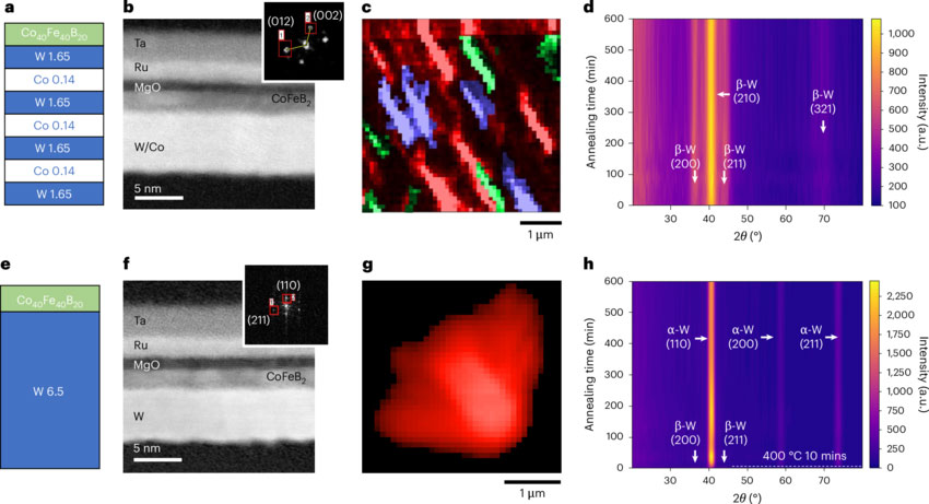
Cobalt too
The research paper reveals that “the insertion of thin layers of cobalt can be used to stabilize β-tungsten under back-end-of-line-compatible thermal conditions.” With the new composite layers, the SOT-MRAM was tested to withstand extreme temperatures (up to 400 °C) for 10 hours, and even 700 °C for 30 mins.
Deliverability and applications
With TSMC scientists among the collaborators, it isn’t surprising to hear that these new SOT-MRAM devices are being designed for large-scale integration under existing semiconductor industry-compatible processes. Almost inevitably, the SOT-MRAM is now being pitched at the AI data center market, as well as low-power computing applications at the edge, where speed and non-volatility will also help spur adoption.

Follow Tom's Hardware on Google News, or add us as a preferred source, to get our latest news, analysis, & reviews in your feeds.