With smaller process nodes becoming increasingly more expensive to achieve, chip manufacturing engineers are turning to other ways to increase the number of transistors that can be packed into a single die. In some ways similar to traditional chip stacking, one research team has created a way to implement an extra layer of microscopic switches on an already completed die, by sticking them where the power and signals go.
Okay, so that's a very rough description of the work conducted by MIT's Department of Electrical Engineering and Computer Science, the University of Waterloo, and Samsung Electronics. But when you read the details about it in the press release on the matter, you'll see that it's a tad difficult to describe it all in just one sentence.
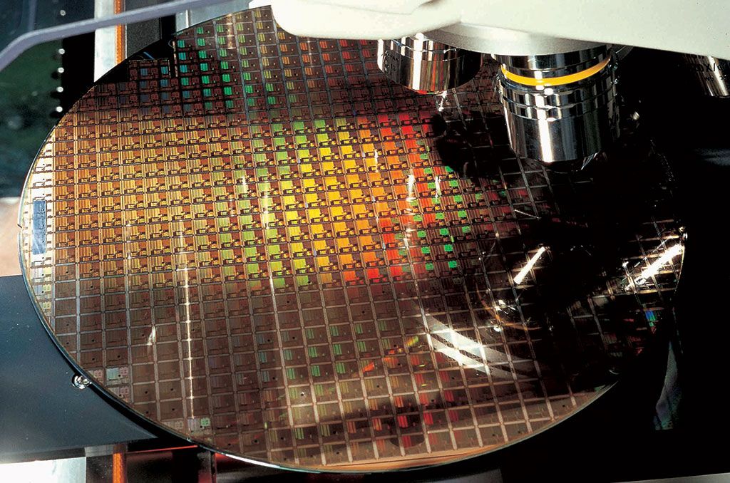
Traditional CMOS chips are fabricated by applying and then etching repeated layers of different materials, applied to a wafer of ultra-pure silicon. The bottom-most layer, also known as the front end according to MIT, comprises the transistors of the chips (or capacities, in the case of DRAM).
However, these need to be fed a current in order to work, plus you need to be able to read and write data to groups of transistors that form logic cells, data registers, and so on. These are made from multiple layers of metals and insulators, aka the back end.
In theory, you can have more than one layer of transistors, but unfortunately, the materials involved are very sensitive to the heat used in the manufacturing process. So much so that any normal process would just destroy the bottom layer as the new one gets applied. Hence, the MIT-led team turned the problem on its head to find a solution.
In other words, they applied a new transistor layer to the back end. But even that's not quite enough to protect the sensitive front end from heat. The researchers solved that problem by using a very thin layer (just 2 nm thick) of amorphous indium oxide for the extra transistors.
It requires a much lower temperature to be applied than traditional materials, which stops the front end from getting damaged. The group also discovered that using a layer of ferroelectric hafnium-zirconium oxide could then be used to create memory cells.
The end result? A chip with a higher transistor density than one without the extra layers. However, don't get too excited just yet. The research is still far from being able to convert all of this into usable circuits at the moment, but all chip architectures start life in this way.
We've already seen researchers discover a way to apply multiple layers of transistors on top of each other, so if processors of the future can be built using both techniques, as well as traditional chip stacking, then the limit to transistor densities will be blown through the roof.
Moore's Law might have looked a bit rocky in recent years, but work like this suggests that rumours of its death are very unfounded.