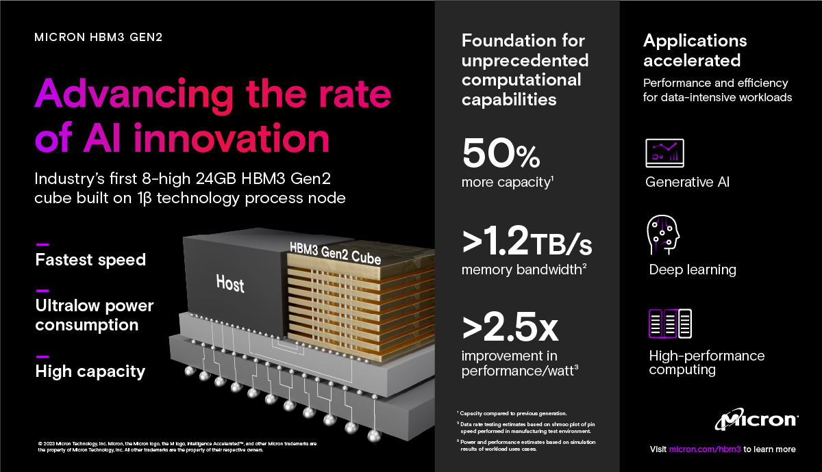
Today Micron announced its new HBM3 Gen2 memory is sampling to its customers, claiming it's the world's fastest with 1.2 TB/s of aggregate bandwidth and the highest-capacity 8-high stack at 24GB (36GB is coming). Micron also claims its new memory is the most power efficient, with a 2.5x improvement-per-watt compared to the company's previous-gen HBM2E. Micron's HBM3 Gen2 also has a 12-high stack option that totals 36GB that's coming 'soon.'
Micron is the first to sample what it terms second-gen HBM3 memory, outstripping rivals like SK hynix and Samsung, which could be an advantage given the current AI arms race that finds vendors scrambling for the fastest and most capacious memory possible to power memory-hungry AI accelerators.

Micron's HMB3 Gen2 offers the highest bandwidth of its memory portfolio. Micron has essentially skipped over releasing a standard HBM3 offering, moving from HBM2E to its 'HBM3 Gen2.' Micron says the new 'Gen2' naming convention is to 'represent the generational leap in performance, capacity, and power efficiency.'
We can also see an 'HBMNext' listed on Micron's roadmap, which could be HBM4. This next-gen memory will deliver 2+ TB/s of throughput and up to 64GB of capacity when it arrives ~2026.

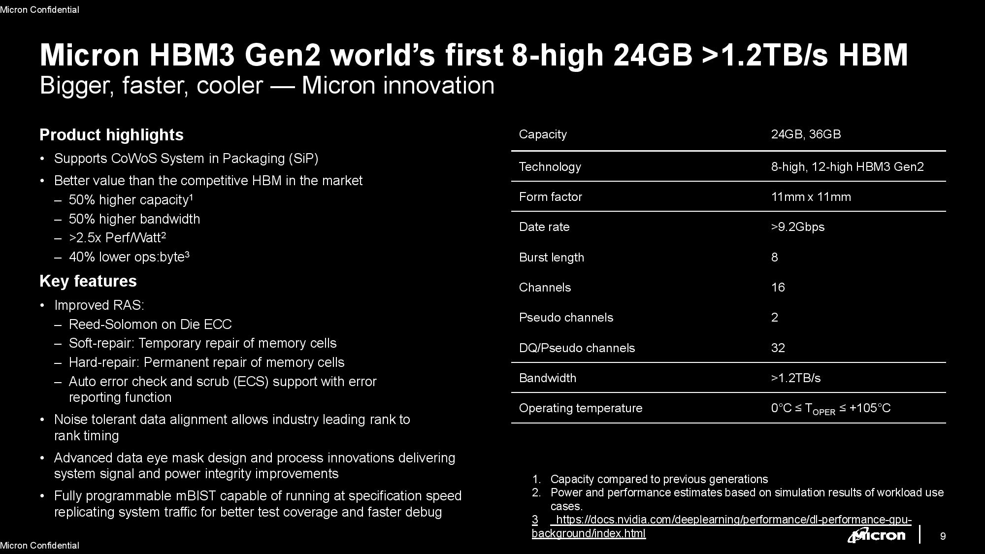
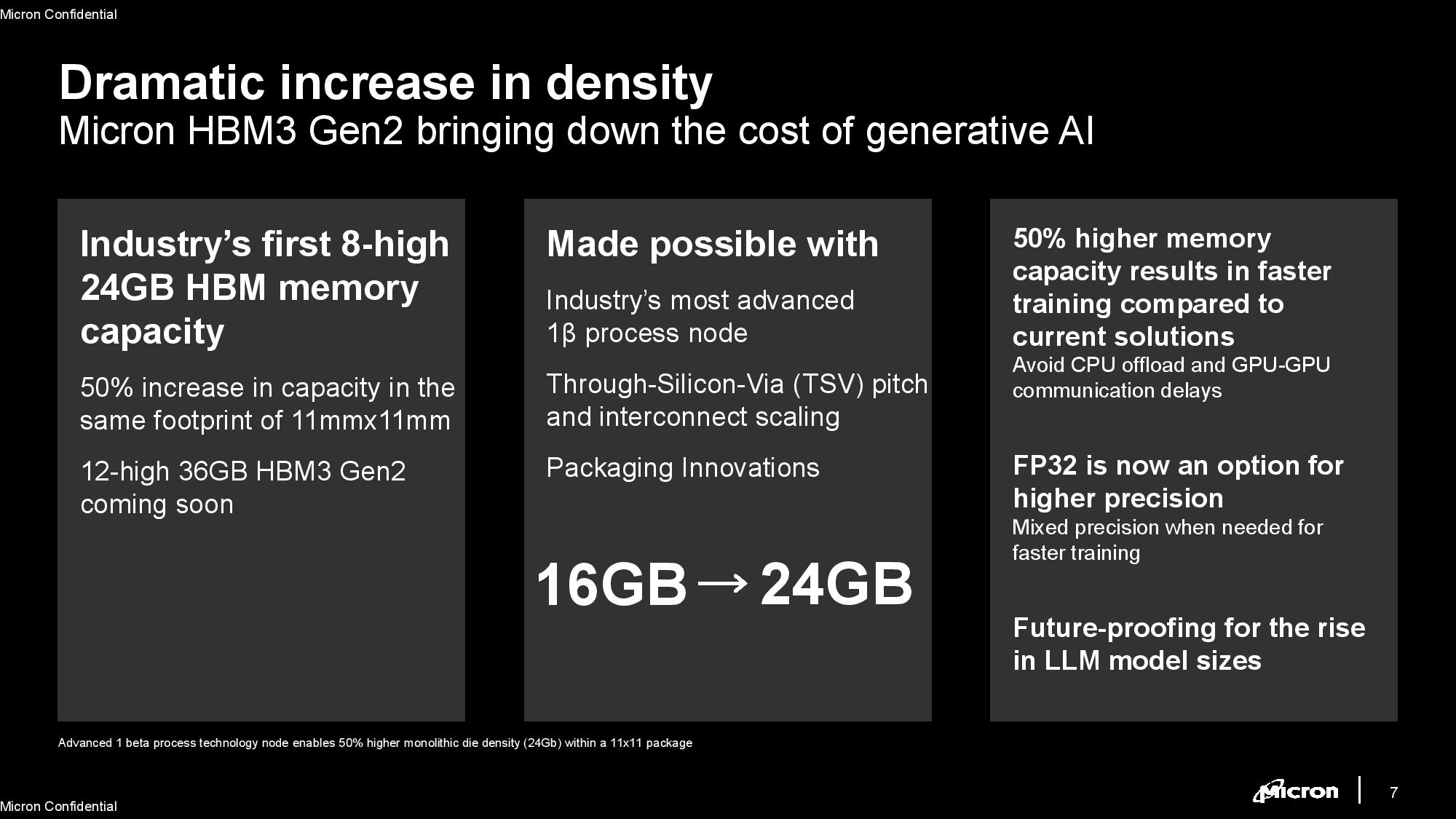


Micron's new HBM3 Gen2 memory has eight stacked 24Gb die (8-high) that provides a 50% capacity increase over other 8-high HBM3 stacks — HBM3 currently tops out at 24GB with a 12-high stack. Micron's new memory also fits into the same 11mmx11mm footprint as standard HBM3, marking a significant density increase. The package is drop-in pin compatible with existing HBM3, making it a relatively easy task to swap in the faster memory.
Micron's HBM3 Gen2 also has a 12-high stack that totals 36GB that's coming 'soon.' For a device with eight HBM packages like AMD's MI300, that would enable up to 288 GB of capacity, while the more-common 6 stacks, like we see with Nvidia's H100, would equate to 216 GB of capacity.
The 8-high stack delivers 50% higher bandwidth with 9.2 Gbps per pin, which works out to 1.2 TB/s with a 1024-bit wide memory bus. That's 50% faster per pin than current HBM3 memory, which tops out at 6.4 Gbps per pin and 820 GB/s of aggregate throughput. Naturally, performance will scale with larger memory subsystems.
It's natural to expect that HBM3 Gen2's higher capacity and bandwidth will result in higher heat, but Micron took several steps to improve thermals to defray potential issues. Micron uses the same 1β (1-beta) process node for HBM3 Gen2 as it uses for its current-gen DDR5 memory. This node, which is Micron's last non-EUV DRAM node, brings with it both density and power efficiency improvements over the memory used for its standard HBM3.
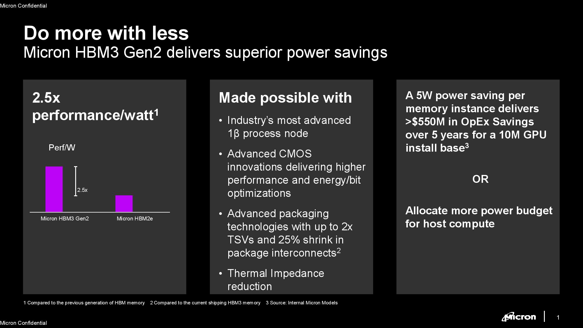
Micron claims that its HBM3 Gen2 delivers a 2.5x improvement in performance-per-watt over its prior-gen HBM2E, and a >50% improvement in Pj/bit (picojoules a bit) over the previous generation (Micron declined to provide a specific number).
Micron reduced the space between the individual DRAM layers by 23%, which helps thermal transfer from the lowest die (which tends to be the hottest) to the top die (which tends to be the coolest). The air between the layers can also have an insulative effect, so reducing the distance between the die has the knock-on effect of reducing the air gap. However, Micron still adheres to the standard 720um Z-height (thickness) of the final package.
Micron also doubled the number of TSVs, which helps improve power efficiency due to increased data lanes, and shrunk the interconnects by 25% compared to current-gen HBM3 (the company declined to share the pitch). The denser metal TSV interconnects also help improve thermal transfer between the layers of the device. Micron also says its HBM3 Gen2 has "a five-time increase in metal density," which also reduces thermal impedance. In culmination, the package fits within the standard 0C to 105C operating range despite the increased capacity and throughput.
Micron says its HBM3 Gen2 has a noise-tolerant design and features advanced signal and power integrity, though Reed-Solomon on Die ECC (error correction code) steps in to correct any issues. Since this is on-die, an extra die isn't required for ECC.
Micron's HBM3 Gen2 package is compatible with standard CoWoS packaging; a must given the industry's preference for this type of packaging for GPUs and other types of accelerators. The HBM3 Gen2 memory has the same channel arrangement as HBM3, with 16 channels and 32 virtual channels (two pseudo-channels per channel).
Micron is the first to ship samples of a second-gen HBM3, but SK hynix recently revealed that it has 24GB HBM3E stacks under development for release in 2024. However, those products are said to peak at 8 Gbps per pin (1TB/s in aggregate), which would give Micron a ~20% advantage in overall bandwidth. Naturally, we'll have to wait for a final announcement from SK hynix before making a more thorough comparison.
Micron's HBM3 Gen2 is sampling to partners now for 8-high stacks, and 12-high stacks will arrive in the near future. High volume production begins in 2024.