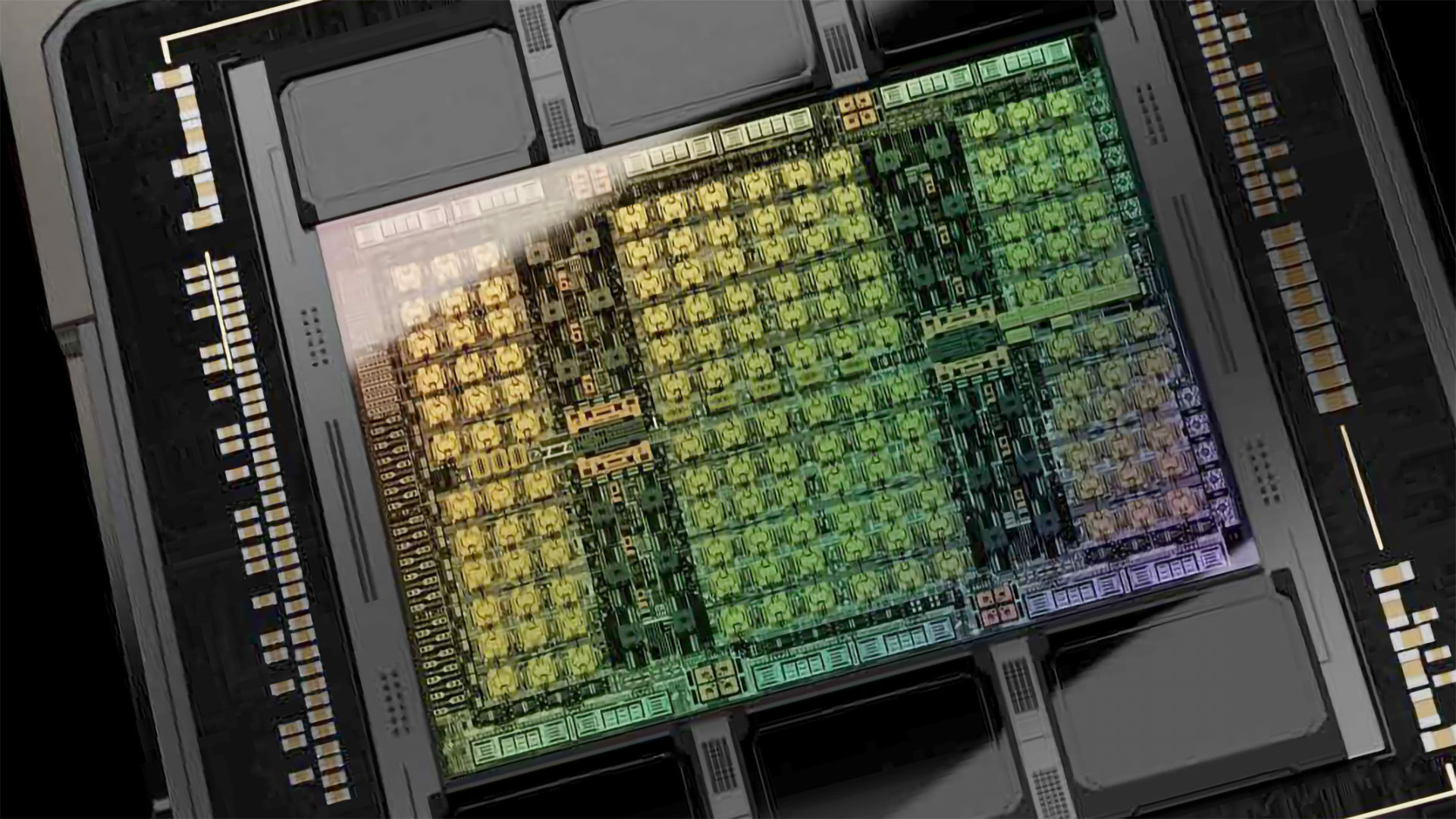
Nvidia's 'Big Blackwell' gaming graphics processor codenamed GB202 will use the same process technology as the recently announced compute-oriented GB200, according to well known hardware leaker @kopite7kimi. It is expected that the new production node will likely offer higher transistor density, so the GB202 will gain the number of execution units.
GB202 will use the same process node as GB100. I must clarify once again that TSMC 4N(vidia) is based on TSMC 5, not 4nm. I'm sorry I cannot match Jensen's naming with TSMC's naming. We need professional chip analysis to determine. At least, there is a 30% increase in density.March 19, 2024
"GB202 will use the same process node as GB200," wrote the leaker who tends to be accurate about Nvidia's future products. They also seemed confident that there would be at least a 30% increase in density.
GB202 will use the same process node as GB100. I must clarify once again that TSMC 4N(vidia) is based on TSMC 5, not 4nm. I'm sorry I cannot match Jensen's naming with TSMC's naming. We need professional chip analysis to determine. At least, there is a 30% increase in density.March 19, 2024
Nvidia's GB100/GB200 processors for AI and HPC workloads rely on TSMC's custom 4NP fabrication process, which is an enhanced version of 4N manufacturing technology developed specifically for graphics processing units. Meanwhile, 4N is a custom version of TSMC's standard N4 production node that belongs to the company's N5-series of 5nm-class technologies.
Considering that Nvidia'a GPUs tend to reuse various building blocks, its not surprising that Blackwell processors for compute and gaming being made on the same manufacturing technology. When it comes to transistor density, there is no way that 4NP has a 30% higher transistor density than 4N. As even N4 can only boast a 6% higher transistor density than N5. Unless 4NP uses some very sophisticated technologies, such as EUV double patterning, to boost transistor density, it is close to impossible to shrink transistor sizes so substantially compared to 4N.
Nvidia's GH100 processor (4N) has a die size of 814 mm^2 and packs 80 billion transistors, so its transistor density is around 98.28 million transistors per mm^2. Nvidia has not yet disclosed the die size of GB200, but something tells us that each of its chiplets should be very close to the reticle size limit, which is 858 mm^2. Assuming that one GB200 chiplet is indeed 858mm2, then its transistor density 121.21 million transistors per mm^2, which is quite an achievement in terms of inter-node transistor density increase.
If we see something similar with the GB202 GPU aimed at gaming market, that would be quite a noticeable improvement. Architectural improvements of Blackwell coupled with increased number of CUDA cores and fixed-function graphics hardware will ensure that Nvidia's next-generation graphics processor for client PCs will have a substantial performance improvement over existing Ada Lovelace GPUs.