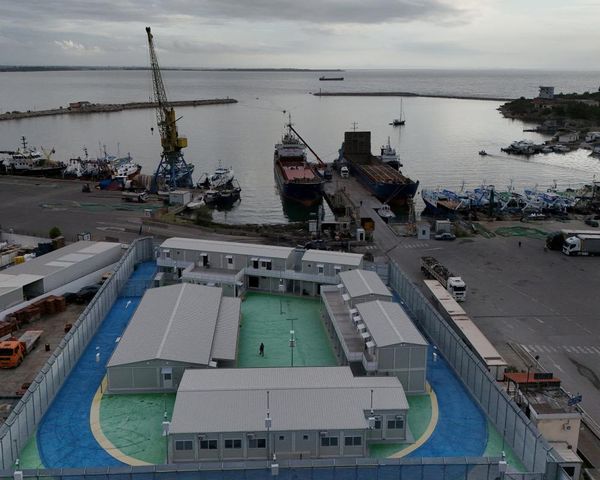
As Intel prepares to move its fabs into its new Intel Foundry business, it will change the way it reports results in the coming months. To discuss the company's long-term vision and give investors a better understanding of how Intel's business will move forward with Intel Foundry and Intel Products groups, Intel plans to host a webinar on segment reporting on April 2, 2024.
"The webinar will discuss the longer-term vision for the foundry business and the importance of establishing a foundry-like relationship between Intel Foundry, Intel's manufacturing organization, and Intel Products, its product business units, to drive greater transparency and accountability," the description of the event reads.
The company plans to submit an 8-K form, revising its past financial reports to align with a new reporting framework, before the upcoming investor webinar. Starting with Q1 FY2024, Intel will disclose its financial outcomes using this new reporting structure.
One of the things that Intel will touch upon at the webinar is the financial and market performance of the Intel Foundry division. These things may not impress. It is likely that initially, Intel Foundry's business will have high costs, and the majority of orders will come from Intel itself (i.e., a significant but still relatively low market share). Meanwhile, Intel Foundry has to invest in advanced fab tools to prep its fabs for 20A and 18A, which drives its costs up, and this likely means losses.
Yet, it will take some time before Intel Foundry obtains revenue streams from major customers, such as Microsoft or the U.S. military. IF's financial numbers and market share may still not impress immediately, but this is normal at this stage. This is perhaps what Intel will communicate and discuss at its upcoming webinar.
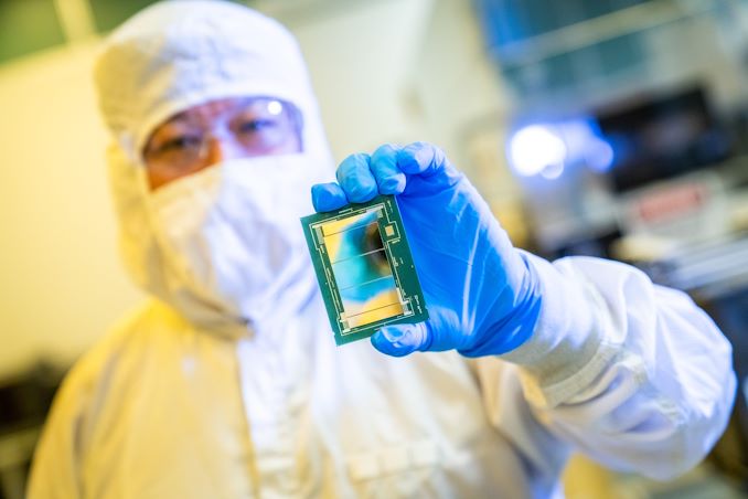
In fact, although Intel fully expects its 18A (1.8nm-class) fabrication process to be ahead of its rivals in terms of power, performance, and area (PPA), the company's chief financial officer reiterated at a conference this week that it does not expect to win the bulk of any large customer's chip orders with this technology.
"We probably will not win anybody's major volume [with] 18A," said David Zisner, CFO of Intel, at the Morgan Stanley Technology, Media, and Telecom Conference (via SeekingAlpha). "We will win some smaller SKUs, and that is all we need, to be honest with you. That will be very significant to us, even though it seems maybe marginal in the marketplace, particularly if we can collect enough of these customers [developing high-performance compute chips]."
Intel's 18A fabrication process builds upon the company's 20A manufacturing technology (a 2nm-class node) that introduces RibbonFET gate-all-around transistors and PowerVia backside power delivery network. In GAA transistors, horizontal channels are fully encased by gates. These channels are built using epitaxial growth and selective removal, enabling adjustments in width for enhanced performance or lower power use. As for the backside power delivery network (BS PDN), the technique moves power lines to the wafer's back, separating them from I/O wiring, which allows for making power vias thicker and reducing their resistance, which helps to both increase transistor performance and lower power consumption.
Both GAA transistors and BS PDN promise to offer significant performance and power efficiency enhancements, which is good for AI, HPC, and smartphone SoCs. Meanwhile, 18A promises a 10% performance per watt improvement over 20A and GAA innovations. Thus, it promises to be quite competitive compared to TSMC's N3B and N3P.
"When it comes to the high-performance compute part of the market, that is really where we are starting to see a lot of our uptake," said Zisner. "The particular aspects of 18A with PowerVia and RibbonFET, combined with our just legacy of experience on high-performance compute, I think, makes us a really compelling partner for customers that are in that space and want to develop products."
Intel's 18A was designed to be a major foundry node, and consequently, its process design kit (PDK) is now available and the production technology is compatible with third-party electronic design automation (EDA) and simulation tools. However, Intel itself does not expect this process to be used for high-volume products of third parties. Even Microsoft is currently only slated to produce one chip on Intel's 18A.
Intel Foundry is a newcomer to the contract chipmaking market. As a result, Intel is planning for a multi-generational effort to break into the market, as the company will need to earn the confidence and business of third-party customers. As this happens, Intel Foundry expects to gain market share and reach profitability.
Sources: Intel, SeekingAlpha