
At ITF World 2023 in Antwerp, Beligum, Ann Kelleher, Intel’s Technology Development GM, presented an outline of Intel’s latest developments in several key areas, and one of the most interesting revelations was that Intel would embrace stacked CFET transistors in the future. This marks the first time that Intel has shown this new type of transistor in its presentations, but Kelleher didn’t provide a date or firm timeline for production.
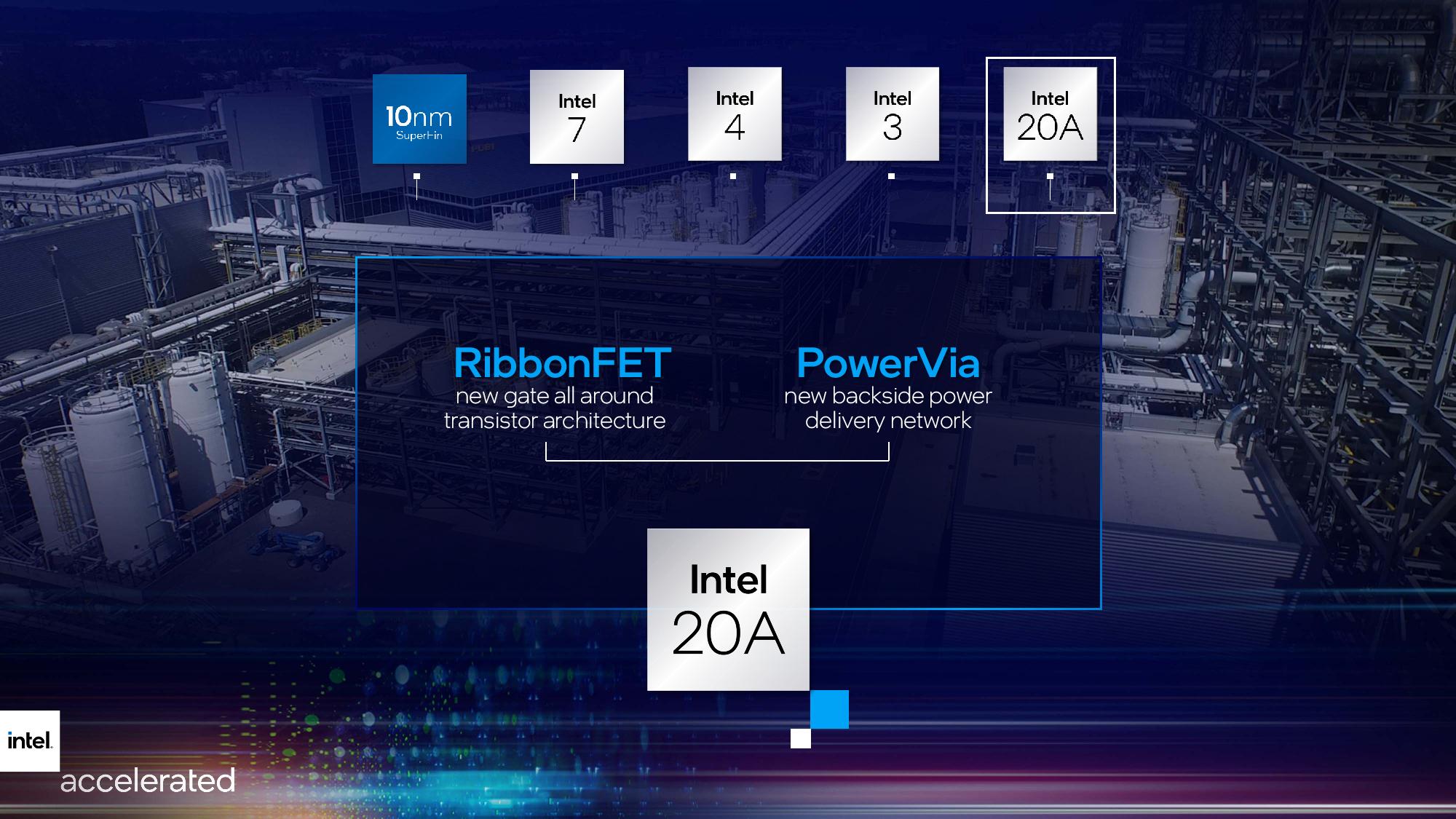
Here we can see a zoomed-in version of the slide with a ring added around the new type of transistor. The first two transistor types at the bottom of the slide are older variants, while the ‘2024’ entry represents Intel’s new RibbonFET transistors that we’ve covered extensively in the past. Intel's first-gen design with the 'Intel 20A' process node features four stacked nanosheets, each surrounded entirely by a gate. Kelleher says this design remains on track to debut in 2024. RibbonFET uses a gate-all-around (GAA) design, which confers both transistor density and performance improvements like faster transistor switching while using the same drive current as multiple fins, but in a smaller area.
Kelleher’s slide also shows the next generation of Intel’s GAA design – the stacked CFET. The Complementary FET (CFET) transistor design has been on imec’s roadmaps for some time, but we haven’t yet seen it on an Intel slide or heard the company state that it plans to adopt this design. As a reminder, the imec research institute studies future technologies and collaborates with the industry to bring them to fruition.
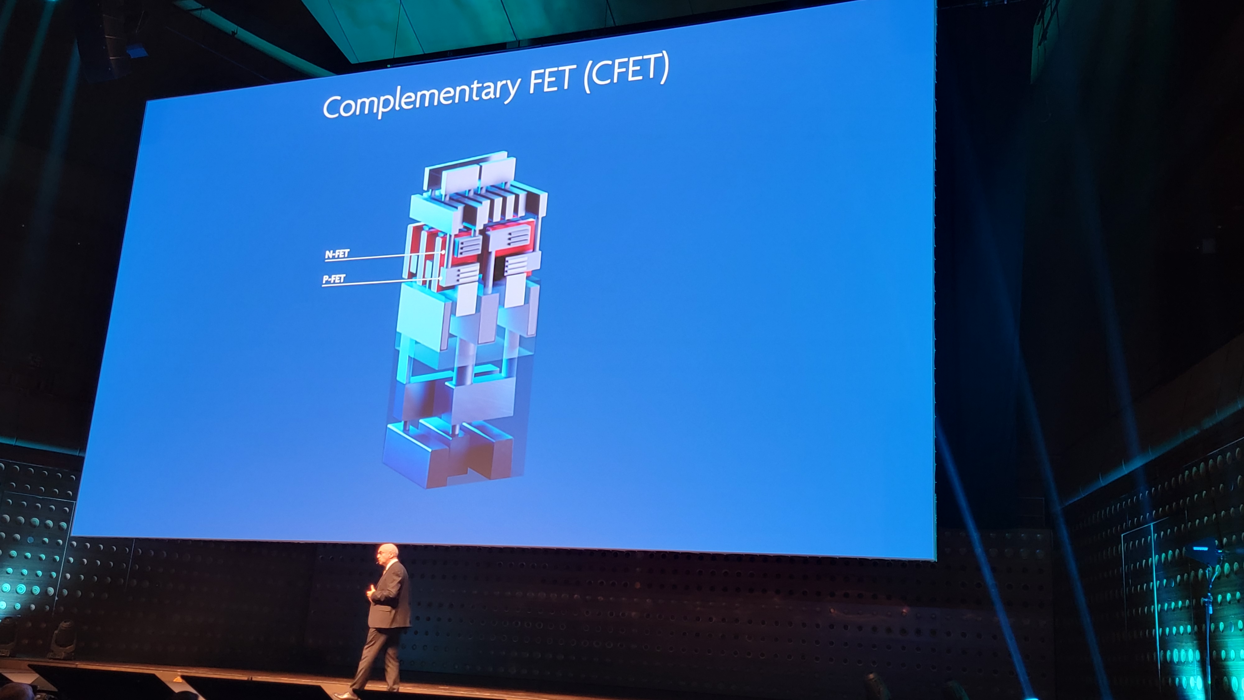
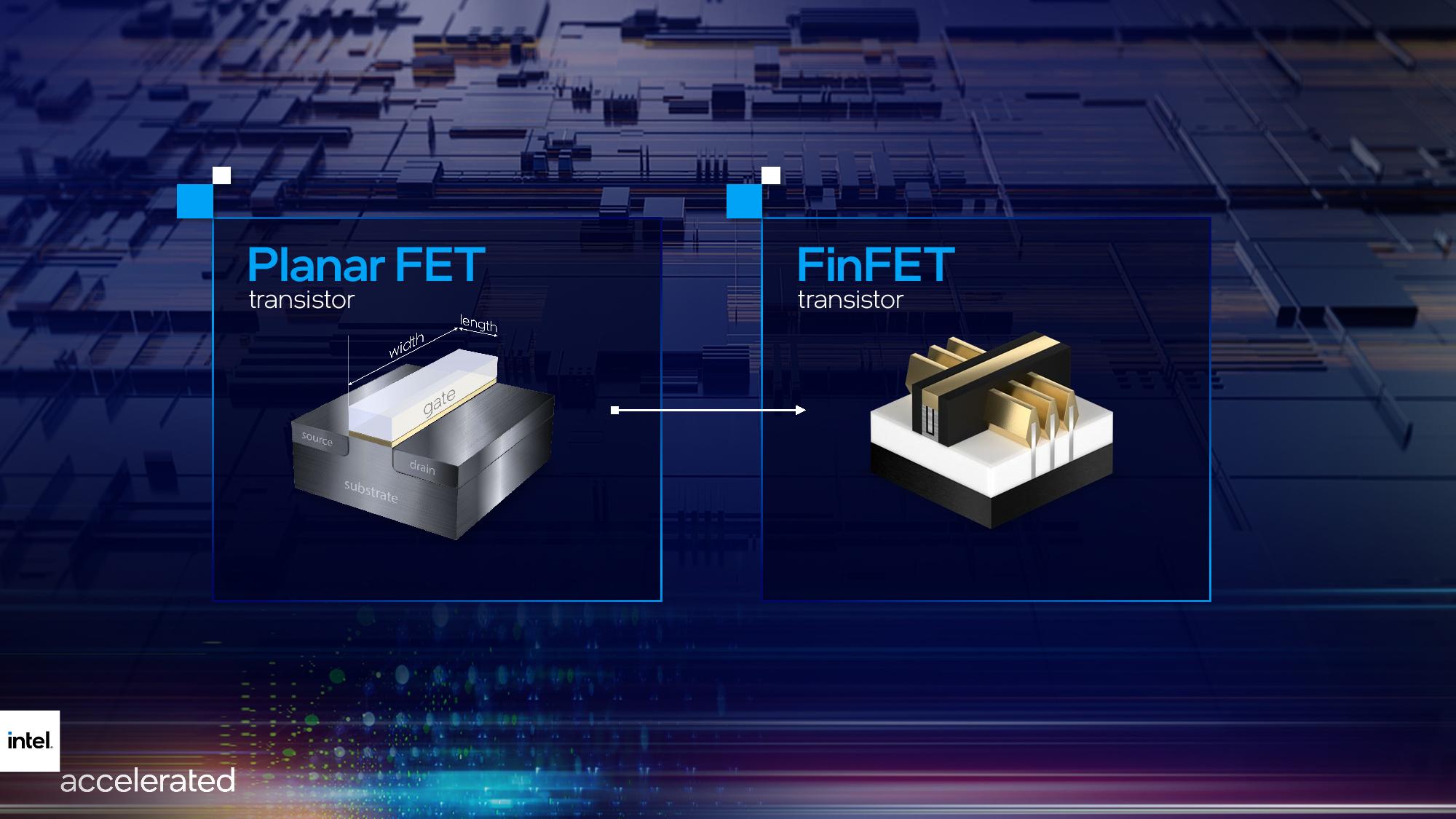

Naturally, there is some variation between Intel’s stylized render and the imec CFET render we’ve included in the first image of the album above, but Intel’s image conveys the point well – this design allows the company to stack eight nanosheets, a doubling of the four used with RibbonFET, thus increasing transistor density. We also have images of the three other types of Intel transistors in the album above — Planar FET, FinFET, and RibbonFET.
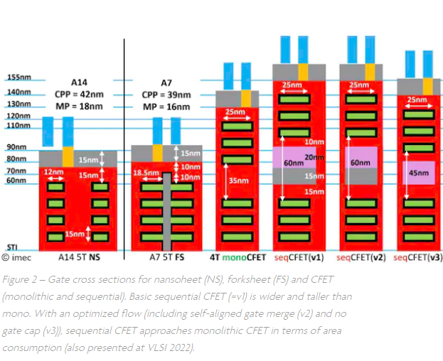
CFET transistors, which you can read more about here, stack n- and pMOS devices atop each other to enable higher density. Two types of CFETs are currently being researched — monolithic and sequential. The four devices on the right side of the above image detail various proposed CFET designs. For now, it is unclear which type of design Intel would adopt, or if it will devise another type of implementation. Given that imec doesn’t have CFETs on its roadmap until around when chips shrink to 5 angstroms in the 2032 timeframe, it could be some time before we find out.
That said, it isn’t guaranteed that Intel would target CFET in that timeframe: Interestingly, Intel’s slide shows its next-gen GAA nanosheet transistor (RibbonFET) and then jumps directly to CFET, omitting the GAA forksheet transistors that most think will be the step between nanosheet and CFET. You can also see that type of transistor in the above slide — it is the second from the left.
Given that Intel’s image isn’t very detailed, it is possible that the company also plans to use forksheet transistors before it moves to CFET, but it hasn’t chosen to share the details yet. We’re following up with Intel to see if we can learn any more details.

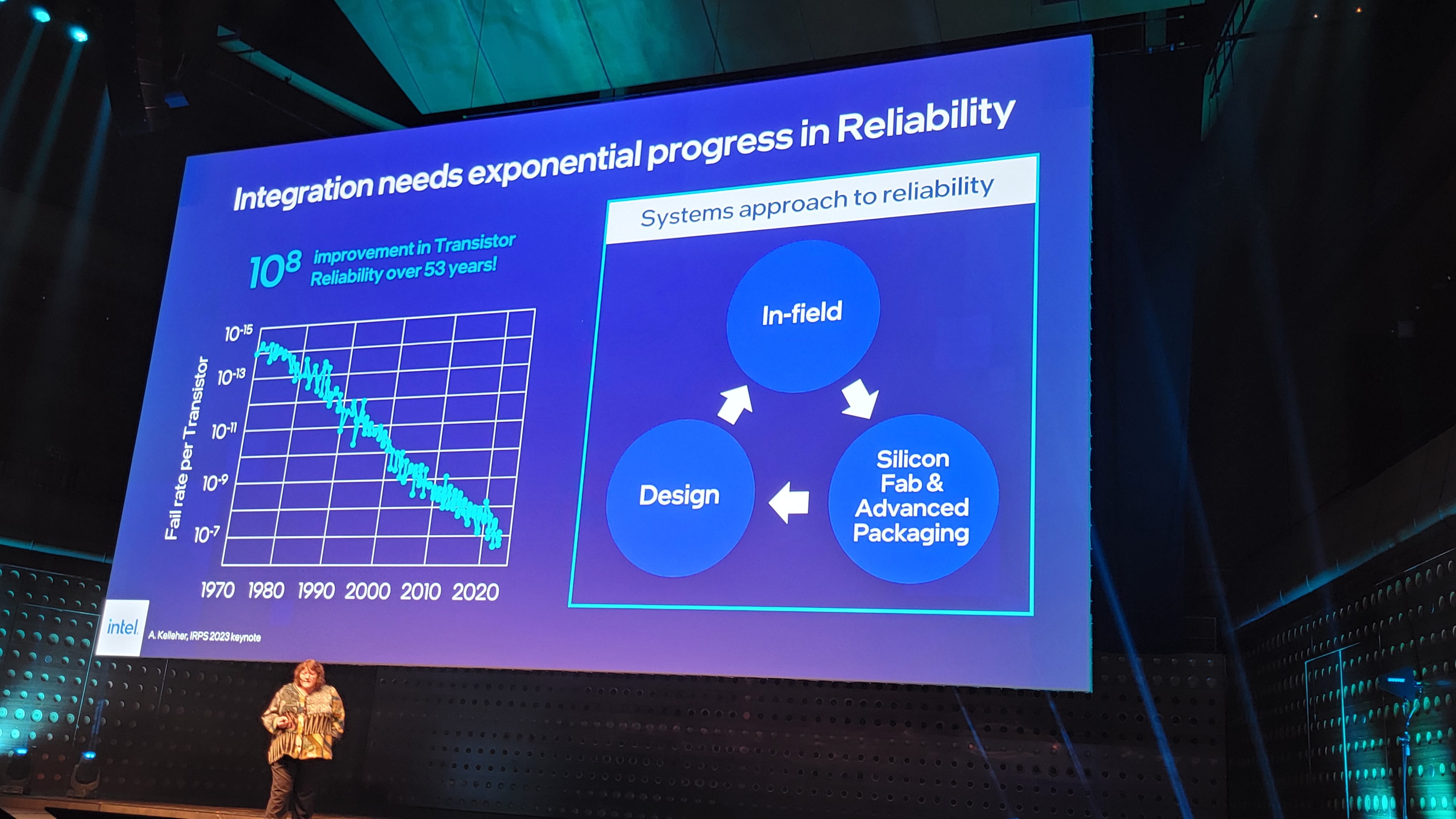
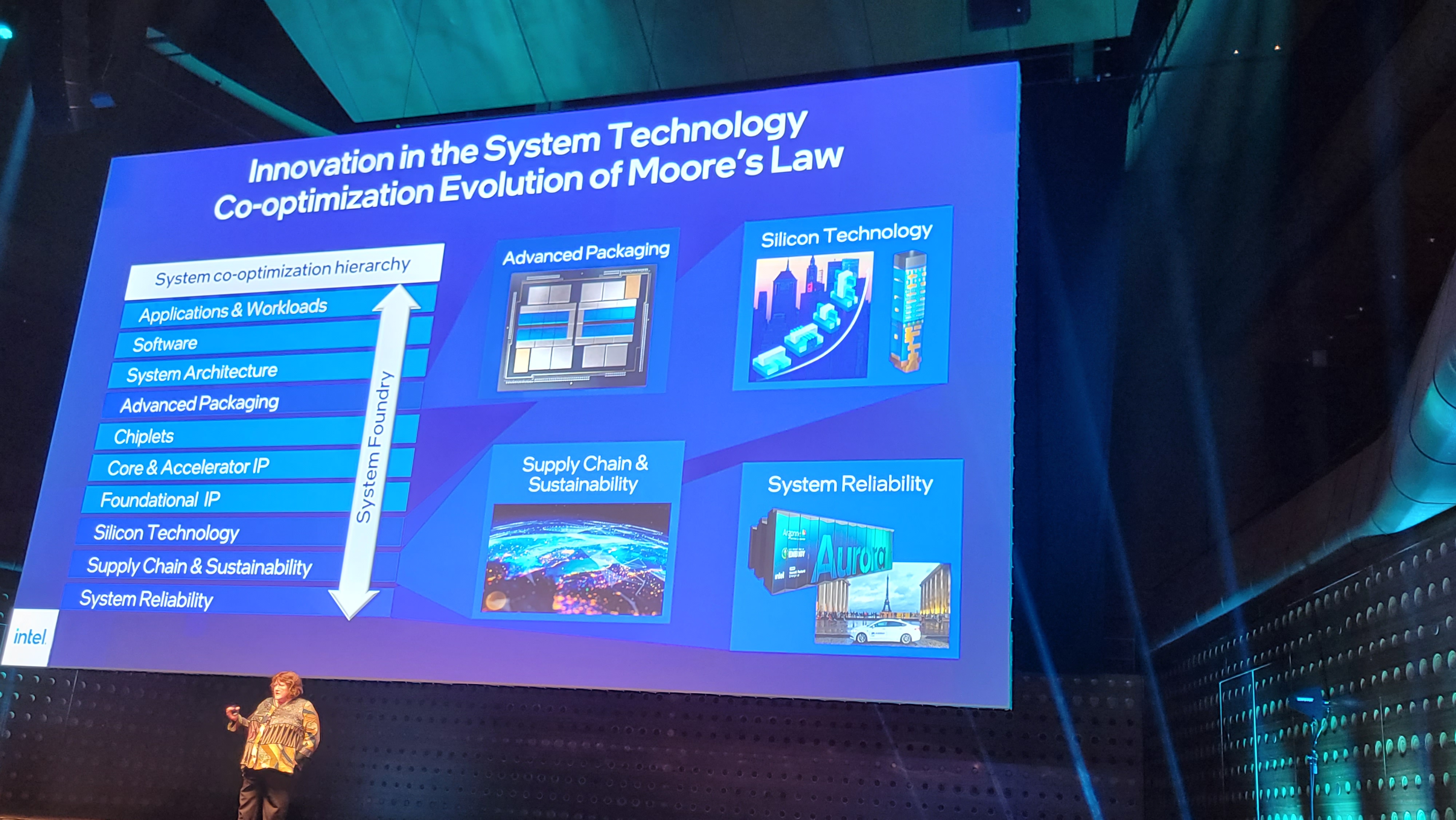

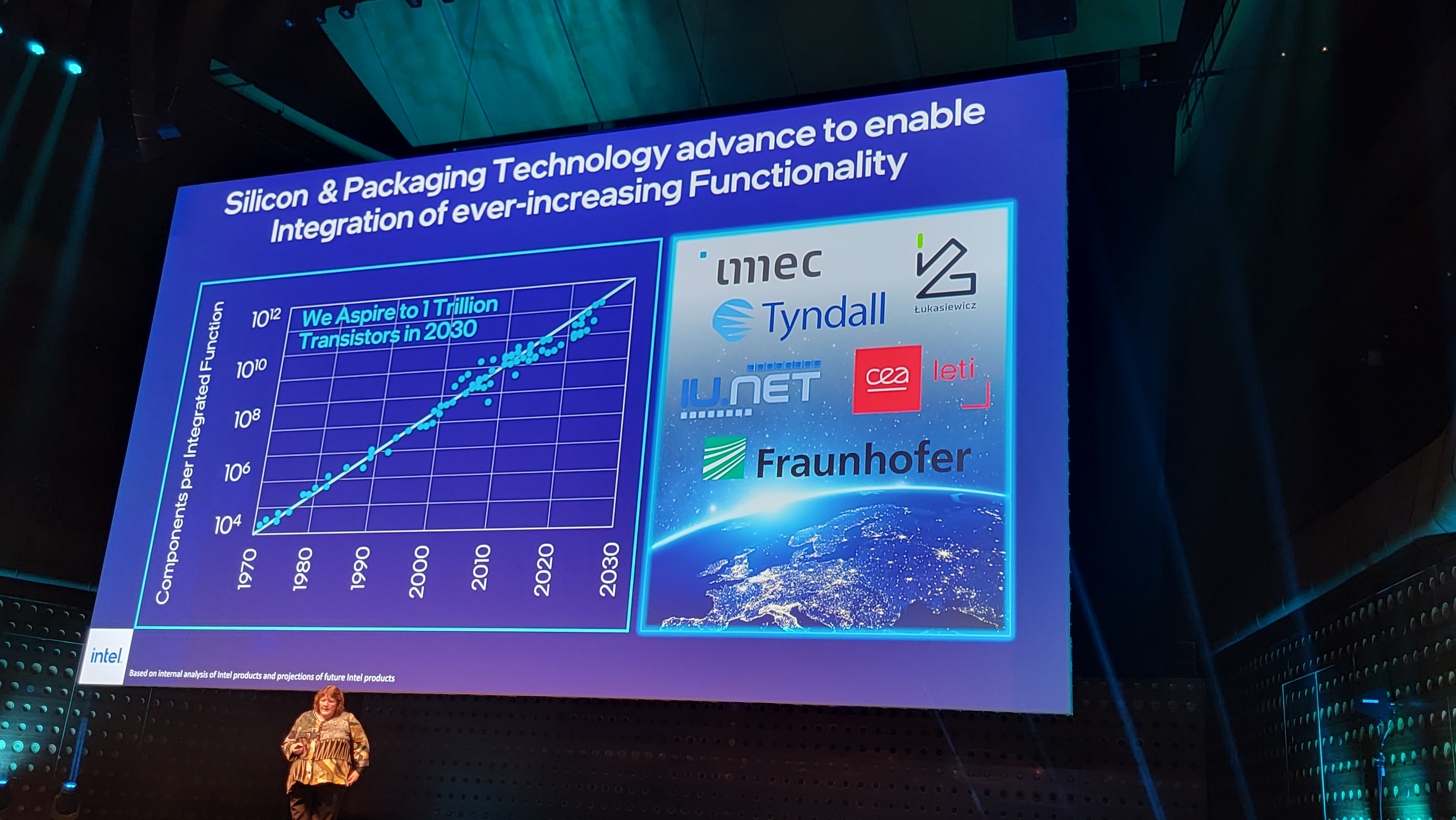


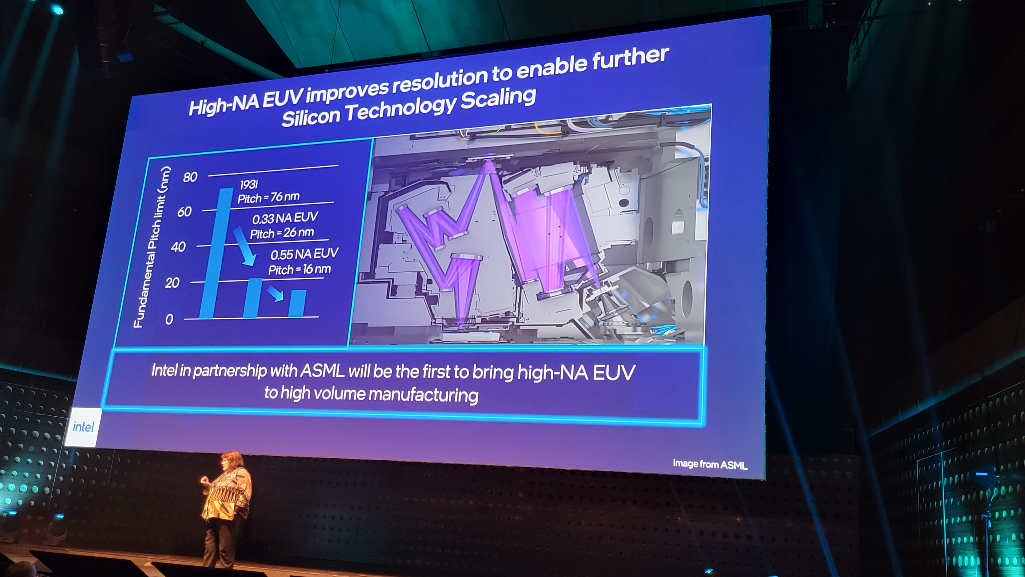
Here are the remainder of the slides from Kelleher’s presentation for your perusal. Kelleher covered a diverse range of topics, including the decline in the cost paid per transistor over time, the increase in the reliability of transistors over time, the increasingly complex packaging process, and the importance of a shift to the System Technology Co-Optimization methodology for Intel's design efforts.
Kelleher’s presentation took place at imec’s ITF World conference, and she opened her speech by reminiscing on her own history with imec – she first worked for imec as a student nearly thirty years ago, eventually spending two years with the research giant. Intel also has a long relationship with imec spanning over the last 30 years, and that work continues today.
You might not be familiar with the Interuniversity Microelectronics Centre (imec), but it ranks among the most important companies in the world. Think of imec as a silicon Switzerland, of sorts. Imec serves as a quiet cornerstone of the industry, bringing fierce rivals like AMD, Intel, Nvidia, TSMC, and Samsung together with chip toolmakers such as ASML and Applied Materials, not to mention the critical semiconductor software design companies (EDA) like Cadence and Synopsys, among others, in a non-competitive environment. This collaboration allows the companies to work together to define the roadmap of the next generation of tools and software they will use to design and manufacture the chips that power the world.