IISc-incubated AGNIT Semiconductors, India’s first vertically integrated gallium nitride (GaN) chipmaker, has set up a new testing and qualification laboratory at IISc, Bengaluru, as it looks to accelerate commercialisation of indigenous technologies.
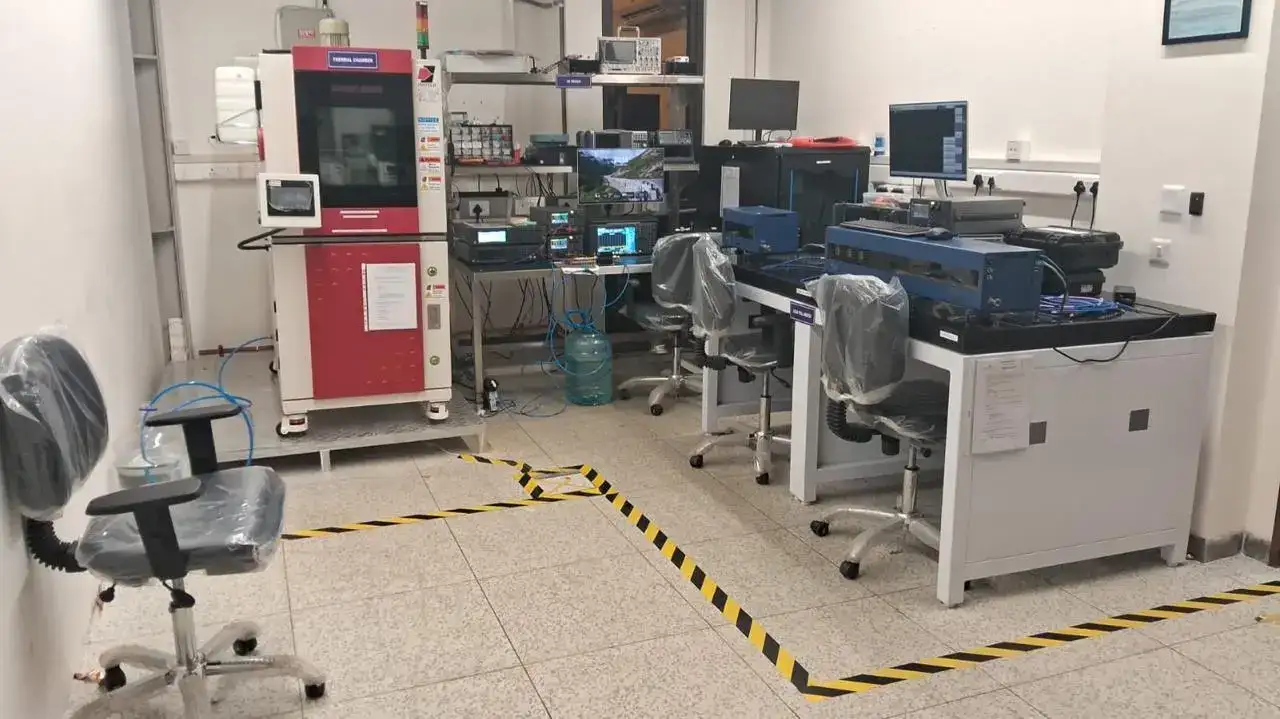
The startup has invested over Rs 3 crore to build the 350 square feet facility, which will focus on in-house validation, reliability testing, and qualification of GaN semiconductor components used in defence, telecom, and next-generation wireless applications.
GaN is a semiconductor material that can handle much higher power, temperature, and frequencies compared to traditional chips, per reports. Unlike conventional silicon, this makes GaN chips more efficient and compact, especially for applications such as defence radar systems, satellite communications, and telecom infrastructure.
The company currently runs five pilot projects with customers, up from three earlier this year. The facility comes as AGNIT prepares for larger commercial orders.
“India’s semiconductor ambitions require not only chip design and fabrication capabilities but also robust indigenous validation and reliability ecosystems,” Hareesh Chandrasekar, cofounder and chief executive of AGNIT, told ET.
The new lab houses infrastructure such as environmental chambers operating between -60°C and 125°C, RF test and measurement benches, connectorised load pull testing stations, and automated PCB assembly systems.
According to Chandrasekar, the facility will significantly reduce testing and product development timelines while giving customers greater confidence in deploying AGNIT’s chips in real-world systems.
“Earlier, we had to work with external vendors, wait for slots, and coordinate testing, which could take three to four months. Now we can do everything in-house in a couple of weeks,” he said. “That significantly improves turnaround times, especially when developing new products, because shorter development cycles allow us to work on more designs simultaneously.
The lab will allow AGNIT to carry out accelerated lifetime testing, stress testing, and reliability qualification for chips operating in high-temperature and high-voltage environments typically seen in defence and telecom systems.
“This facility gives customers the assurance that we can test our chips to their specifications in their end-use environment and provide qualification data, so they can integrate our components into systems,” Chandrasekar said.
He added that while semiconductor foundries can perform basic testing, they cannot validate components in the actual application-specific environments where the chips are ultimately deployed.
Founded on more than 15 years of research at IISc, AGNIT designs and manufactures radio-frequency GaN semiconductor components, the company said. The company has so far raised around $7.47 million to date from investors including 3one4 Capital and Zephyr Peacock, with participation from former Cognizant chief executive Lakshmi Narayanan.
The startup has a team of 34 employees and expects to expand to around 40 in the coming months, Chandrasekar said. It aims to produce nearly 100,000 chips over the next 24 months.
“The long-term goal has always been to build a complete Indian gallium nitride ecosystem, from design and manufacturing to packaging and delivering modules and solutions to customers,” Chandrasekar said.