
EDIT 11/05/2023 7:05am PT: Corrected miscalculations of the performance values stated in the article.
Original Article:
A new paper from Tsinghua University, China, describes the development and operation of an ultra-fast and highly efficient AI processing chip specialized in computer vision tasks. The All-analog Chip Combining Electronic and Light Computing (ACCEL), as the chip is called, leverages photonic and analog computing in a specialized architecture that’s capable of delivering over 3.7 times the performance of an Nvidia A100 in an image classification workload. Yes, it’s a specialized chip for vision tasks – but instead of seeing it as market fragmentation, we can see it as another step towards the future of heterogeneous computing, where semiconductors are increasingly designed to fit a specific need rather than in a “catch-all” configuration.
As noted in the paper published in Nature, the simulated ACCEL processor hits 4,600 tera-operations per second (TOPS) in vision tasks. This works out to a 3.7X performance advantage over Nvidia’s A100 (Ampere) that's listed at a peak of 1,248 TOPS in INT8 workloads (with sparsity). According to the research paper, ACCEL can has a systemic energy efficiency of 74.8 peta-operations per second per watt. Nvidia’s A100 has since been superseded by Hopper and its 80-billion transistors H100 super-chip, but even that looks unimpressive against these results.
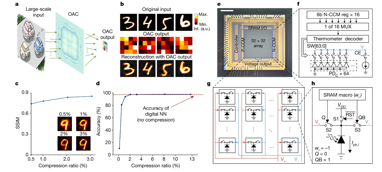
Of course, speed is essential in any processing system. However, accuracy is necessary for computer vision tasks. After all, the range of applications and ways these systems are used to govern our lives and civilization is wide: it stretches from the wearable devices market (perhaps in XR scenarios) through autonomous driving, industrial inspections, and other image detection and recognition systems in general, such as facial recognition. Tsinghua University’s paper says that ACCEL was experimentally tried against Fashion-MNIST, 3-class ImageNet classification, and time-lapse video recognition tasks with “competitively high” accuracy levels (at 85.5%, 82.0%, and 92.6%, respectively) while showing superior system robustness in low-light conditions (0.14 fJ μm−2 each frame).
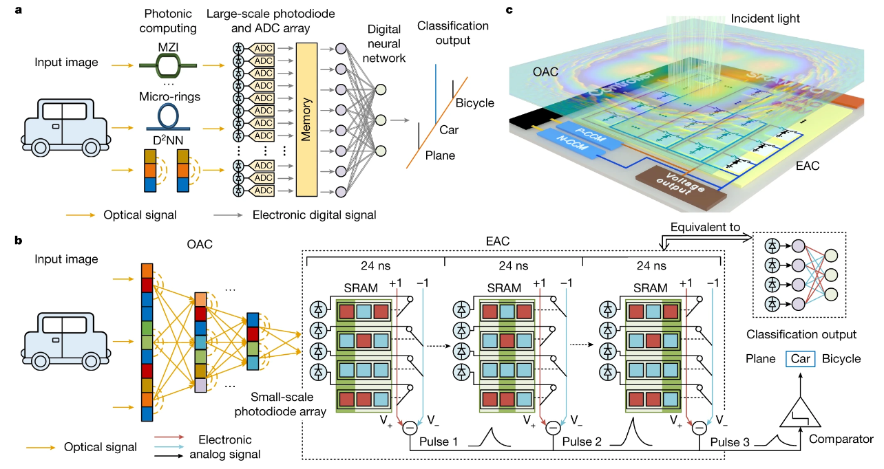
In the case of ACCEL, Tsinghua’s architecture operates through diffractive optical analog computing (OAC) assisted by electronic analog computing (EAC) with scalability, nonlinearity, and flexibility in one chip – but 99% of its operation is implemented within the optical system. According to the paper, this helps in fighting constraints found in other vision architectures such as Mach–Zehnder interferometers and diffractive Deep Neural Networks (DNNs).
That 99% number is relevant to explaining at least the disparity in energy efficiency between ACCEL and other non-analog approaches: Nvidia’s GPU is 100% digital, meaning that its operation is based on the continuous flow of electrons (and produces waste heat as a result).
A photonic, optical system, however, leverages non-electrical ways of transferring, operating on, and encoding information. This can be done via laser pulses at specific wavelengths (we explored this in our recent article on China’s Quantum Key Distribution [QKD] satellite system, also photonic-based) being used to extract and communicate features of visual data (an image) and operating on that light (changing it) virtually on-transit. As a result of this optical processing system, there are fewer energy requirements and electrons wasted in thermal dissipation. Getting rid of the high energy and latency cost of ADCs (Analog-to-Digital Converters) goes a long way toward the performance improvements unlocked by photonics. It’s also why photonics systems are used across quantum computing and HPC (High-Performance Computing) installations.
Simultaneously, we reap speed benefits from moving away from the orderly but messy movement of electrons across semiconductors and unlock operating speeds limited only by light itself. As a result, the research paper claims in-house tests of the chip showcased a low computing latency of each frame at 72ns – resulting in a throughput of approximately 13,000 frames generated per second, more than enough to make any Doom player lose track of reality. It also seems like there would be enough frames for a co-processor to analyze a selection of those images in any computing-vision task. It hardly seems like the deep learning processing of these images through ACCEL would be the bottleneck.
ACCEL seems to be an analog rendition of an Application-Specific Integrated Circuit (ASIC) design. That’s precisely the role of the electronic analog computing (EAC) unit, as it can reconfigure the analog pathways within it to accelerate specific tasks. Think of these as pre-programmed algorithms within the chip, with the EAC coordinating which configuration should be applied to which task.
Dai Qionghai, one of the co-leaders of the research team, said, “Developing a new computing architecture for the AI era is a pinnacle achievement. However, the more important challenge is to bring this new architecture to practical applications, solving major national and public needs, which is our responsibility.”
The new ACCEL chip being photonic and analog may bring to mind the recent IBM announcement of another analog AI-acceleration chip (Hermes). It’s perhaps interesting to witness how even with all sanctions being applied to China, the country’s research and development is allowing it to catch up – and in some ways, apparently improve upon – whatever it was that they were being impeded of. Being able to go around limitations is undoubtedly the way China is thinking about sanctions.
It’s also important to understand that this generation of photonics-based analog chips is being worked on at extremely relaxed lithography levels. ACCEL, for instance, was manufactured on a standard 180-nm CMOS technology for the Electronic Analog Computing unit (EAC) – the brains of the operation. Naturally, further efficiency improvements could be gained from further miniaturizing the process towards lower CMOS nodes (Nvidia’s H100 is fabricated at a 4 nm process). It’s unclear what further work can be done to miniaturize the Optical Analog Computing (OAC) module.
It seems that implementing analog computing systems such as ACCEL at scale is more of a question of fabrication throughput and industry adaptation rather than of physical impossibility. But there’s a reason high-performance AI analog chips still haven’t been deployed at scale: their manufacturing is currently too low to serve anything other than research efforts and prototypical work. We now don’t have the throughput nor the available capacity to add these chips to the already-commited-through-2025 manufacturing commitments at companies such as TSMC – but these experimental results are always needed before committing to scale anything. And the markets meant for chips such as these would very much like to have them. Ultimately, it’s all a matter of planning, spending, and time.