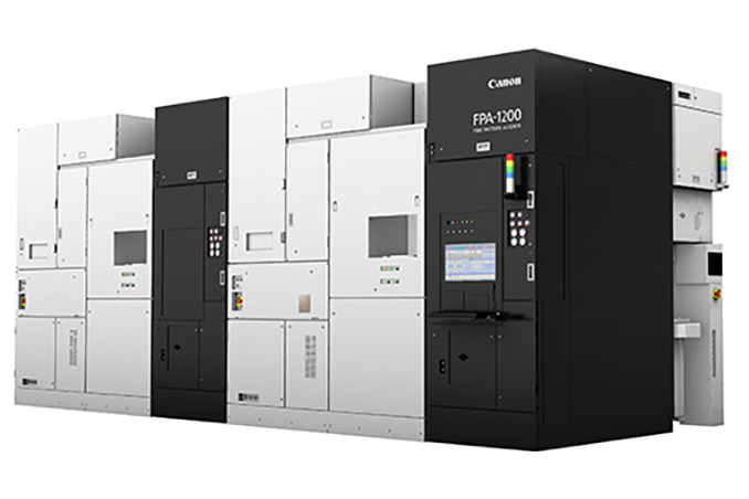
Canon recently introduced its nanoimprint lithography (NIL) tool that can be used to make chips on a 5nm-class process technology, and compete against ASML's extreme ultraviolet (EUV) lithography tools. Apparently, Canon is looking to price its tool at a fraction of that of ASML's EUV litho machines, which could democratize access to advanced chip production for smaller chipmakers without vast resources, according to Bloomberg.
"The price will have one digit less than ASML's EUV [litho tool]," said Fujio Mitarai, chief executive of Canon, in an interview with Bloomberg. " I do not expect nanoimprint technology to overtake EUVs, but I’m confident this will create new opportunities and demand. We are already fielding many inquiries from customers."
Today's EUV systems with a 0.33 numerical aperture cost more than $150 million. Canon implies that its NIL lithography machine will cost around $15 million, which will open doors for smaller companies to make chips on advanced production nodes. However, the final pricing is yet to be determined and even Canon itself does not believe that nanoimprint lithography will replace traditional EUV and DUV scanners.
Conventional deep ultraviolet (DUV) and extreme ultraviolet (EUV) photolithography systems project a circuit pattern onto a resist-layered wafer using a special photomask. By contrast, nanoimprint lithography (NIL) utilizes a mask (or rather a mold) that has been patterned with the circuit design, which is then directly stamped onto the resist on the wafer. This stamping method bypasses the need for an optical system to transfer the pattern, which may lead to a more precise replication of the complex circuit designs from the mold to the wafer. Theoretically, NIL can create intricate two-dimensional or three-dimensional circuit patterns in a single step, potentially reducing production costs as well. There is a catch though. While photolithography allows the processing of entire wafers at once (albeit in multiple steps) NIL is a serial process and may be slower.
Furthermore, a significant concern for NIL is its tendency to pick up defects because of the direct contact between the mold and the substrate during the imprinting step. Any particles or impurities on either the mold or the substrate can introduce flaws, potentially compromising the manufacturing process's yield and dependability. Avoiding this requires stringent process management and an ultra-clean environment to ensure a uniform quality of production.
Canon's entry into the market comes at a time when geopolitical tensions have led to a ban on the export of ASML's EUV and advanced DUV systems to China. This embargo has inadvertently created a potential niche for Canon's new offerings, which were not explicitly included in Japan's tightened chipmaking export controls implemented in July. But the head of Canon believes that the company will still be unable to ship its tool to China since it allows for the production of chips below 14nm, and such tools may require export licenses from the Japanese government.
"My understanding is that exports of anything beyond 14nm technology is banned, so I do not think we will be able to sell," said Mitarai.