ASML on Thursday announced that it had begun shipping the industry's first extreme ultraviolet (EUV) lithography tool with a 0.55 numerical aperture (High-NA) to Intel. The initial High-NA machine will be used to learn how it works on Intel's 18A (18 angstroms, 1.8nm-class) fabrication process, which promises to provide the CPU giant a lead over its rivals TSMC and Samsung.
"We are shipping the first High NA system and announced this in a social media post today," a spokesperson for ASML said. "It goes to Intel as planned and announced earlier."
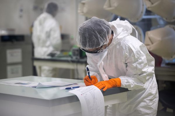
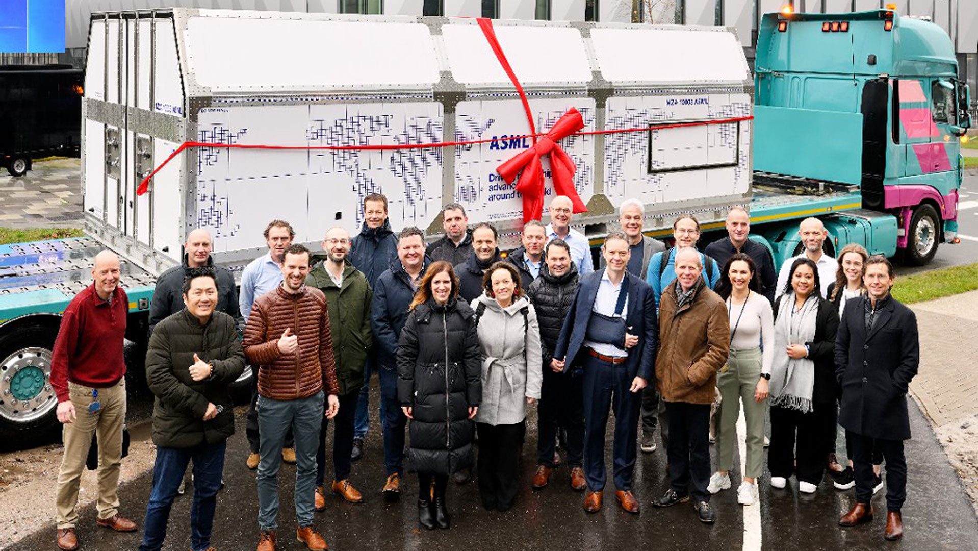
As announced in September, ASML this week began to (literally) ship its High-NA EUV lithography tool to Intel. The unit will be shipped from Veldhoven, the Netherlands, to Intel's site near Hillsboro, Oregon, and will be installed there over the next few months. The machine is so big that it takes 13 huge containers and 250 crates to ship it. It is believed that each High-NA EUV scanner costs somewhere around $300 to $400 million.
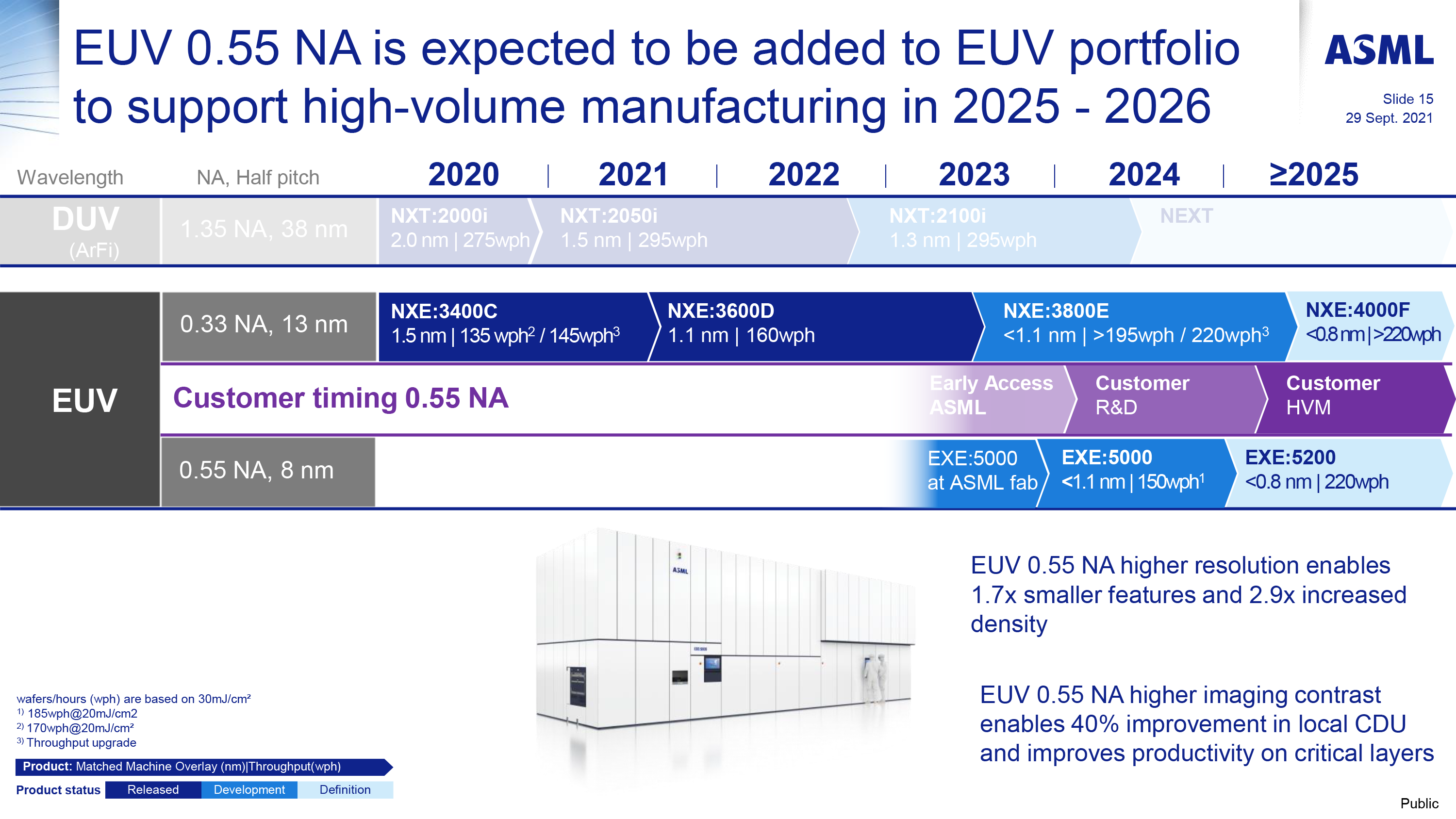
The High-NA EUV tool that ASML ships is pilot Twinscan EXE:5000 machine which Intel acquired in 2018. This unit will be used by Intel to better learn high High-NA EUV tools work on its 18A process technology and gain valuable experience before the company will deploy commercial-grade Twinscan EXE:5200 machines for high-volume chip manufacturing beginning in 2025 using a post-18A production node.
High-NA EUV lithography tools equipped with a 0.55 NA (High-NA) lens can achieve a resolution of 8nm, a notable advancement over standard EUV tools with a 0.33 NA (Low-NA) lens that offer a 13nm resolution. High-NA technology are projected to play a crucial role for post 2nm-class process technologies that will either need to use Low-NA EUV double patterning or High-NA EUV single-patterning.
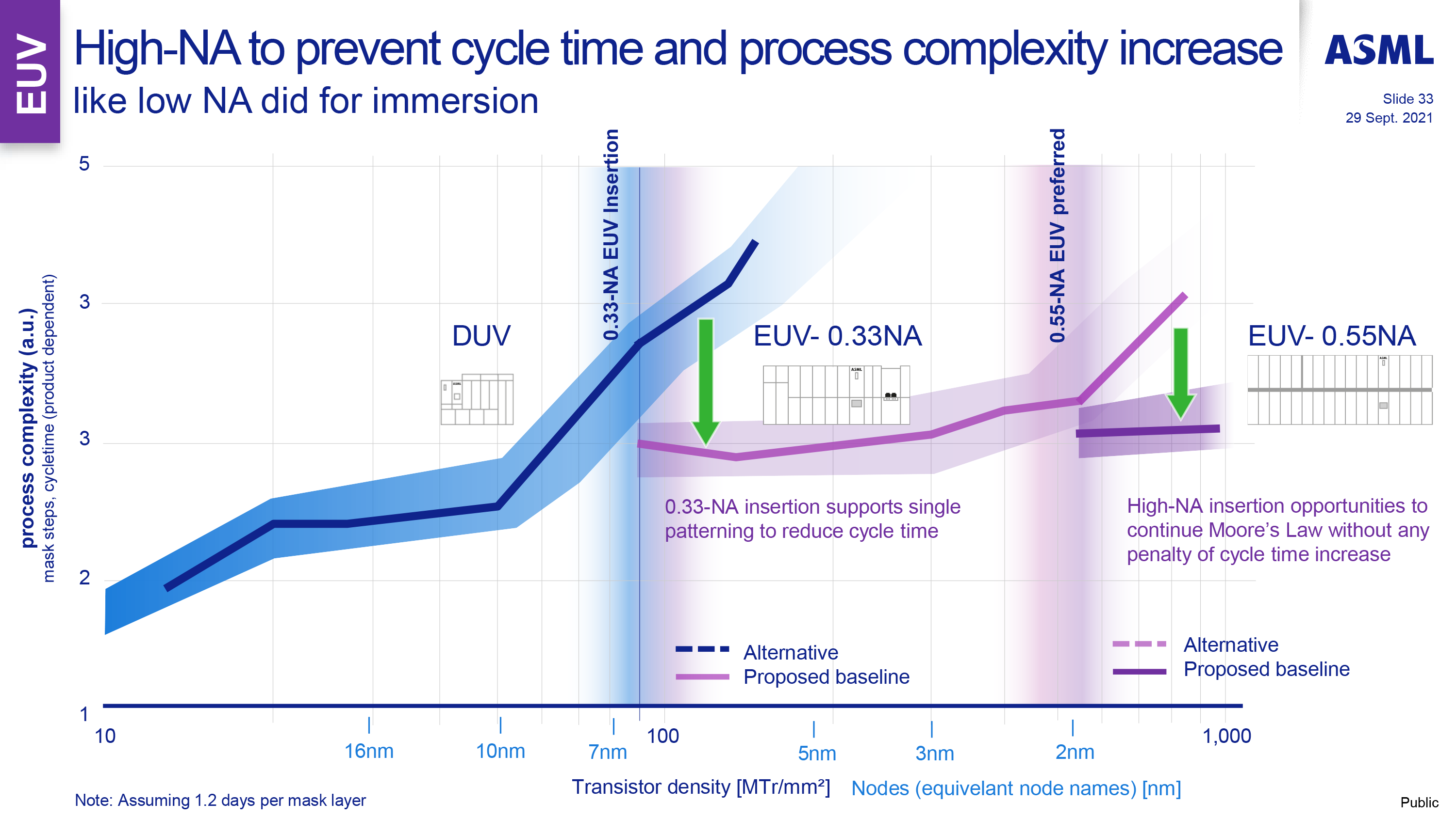
Since High-NA lithography tools have a number of differences with Low-NA litho machines that will require a lot of infrastructural changes, deploying a Twinscan EXE quarters ahead of its rivals could be a huge advantage for Intel. On the one hand, Intel will have plenty of time to adjust its post-18A process technologies. On the other hand, the company will adjust High-NA infrastructure for itself, which will give it another advantage over its competitors.