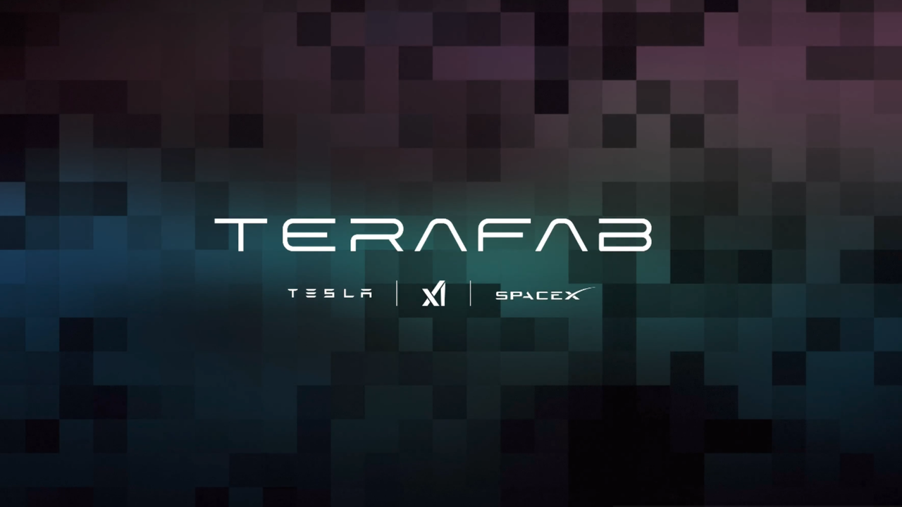
ASML CEO Christophe Fouquet said on Wednesday that he has spoken directly with Elon Musk about the TeraFab semiconductor project, telling Reuters that the SpaceX and Tesla founder is "very serious" about building one of the largest chip manufacturing operations ever attempted.
Fouquet, speaking at a tech event in Antwerp, Belgium, also warned that soaring AI demand will leave the global semiconductor industry short on capacity for the foreseeable future.
Go deeper with TH Premium: AI and data centers
- Photonics and high-speed data movement is the next big AI bottleneck
- The data center cooling state of play
- Massive AI data center buildouts are squeezing energy supplies
- Ultra Ethernet: The data center interconnection of tomorrow
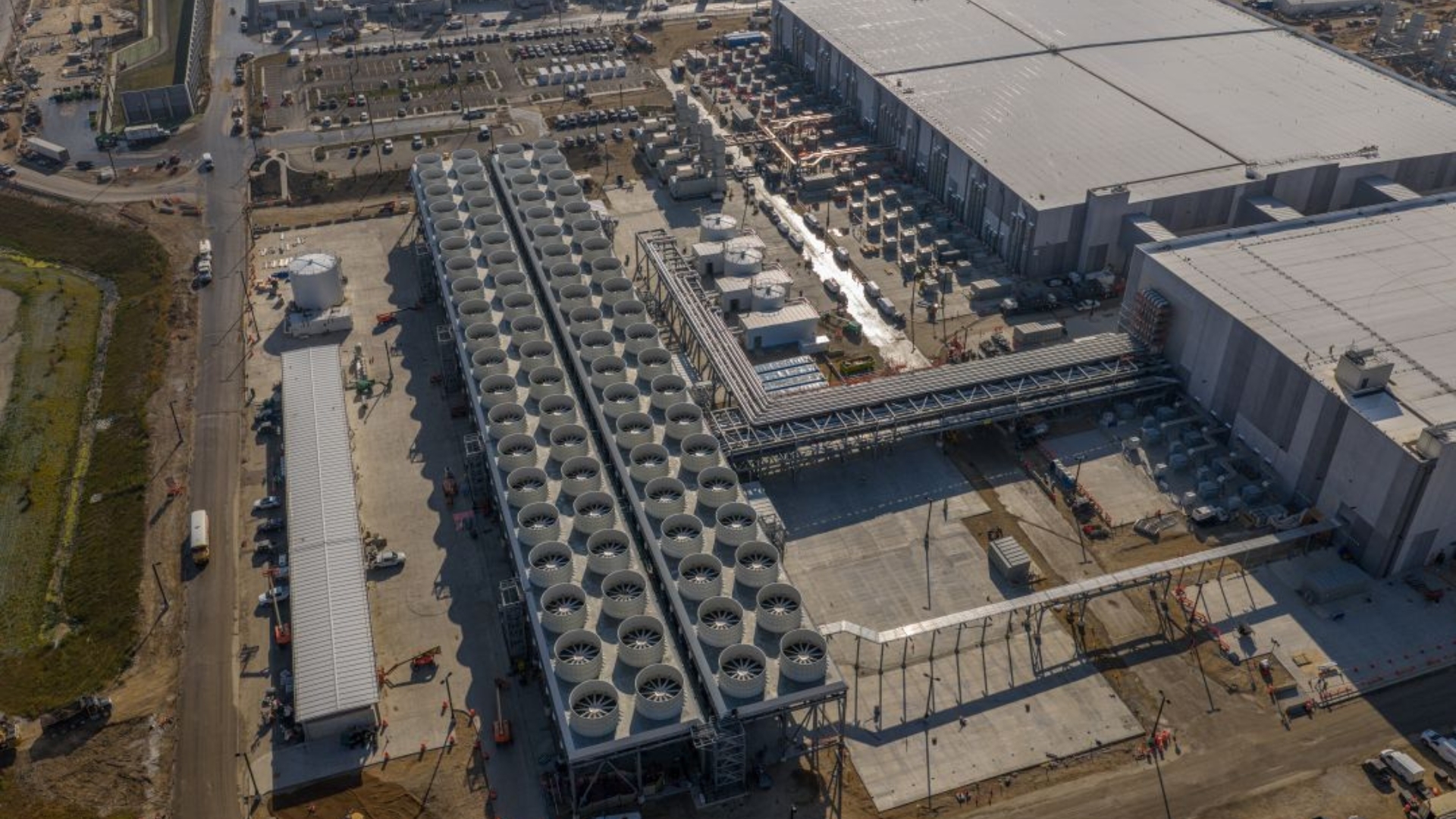
TeraFab, which Musk announced in March with an initial $20 billion investment, will aim to produce logic chips, memory, and advanced packaging under one roof in Texas. Intel joined the project in April and plans to contribute its 14A process technology, and SpaceX has since filed for a $55 billion semiconductor facility in Grimes County, Texas, with potential expansion costs reaching $119 billion.
Fouquet didn’t share details of his conversations with Musk but said that projects like TeraFab and Starlink would put pressure on equipment makers' capacity over the coming years.
ASML is the sole global supplier of EUV lithography systems, which are required to manufacture any chip at the leading edge. Any serious new entrant to advanced chipmaking, TeraFab included, would need to procure billions of dollars in ASML equipment. The company currently has orders from every major foundry and memory maker, including TSMC, Samsung, SK Hynix, Micron, and Intel.
Fouquet says that he expects the first logic chips produced with ASML's High NA EUV lithography systems to arrive within months. Intel is the earliest adoptee, having installed and completed acceptance testing of its Twinscan EXE:5200B at the D1X fab in Oregon late last year. The High NA tools use a 0.55 numerical aperture lens, enabling roughly 2.9 times the transistor density of current EUV systems in a single exposure.
Fouquet also confirmed that ASML is developing a second advanced packaging tool, expanding the company's product line beyond lithography. He described the segment as “a small leg” right now, but added that it will present new opportunities for ASML.
On export controls, Fouquet pushed back against the proposed MATCH Act, which U.S. lawmakers introduced last month to ban sales and servicing of ASML's DUV lithography tools to Chinese customers, among other things. He noted that the DUV immersion systems ASML currently sells to China are based on tech first introduced in 2015, placing them eight generations behind the leading edge. Further restrictions, he argued, would only speed up China's domestic efforts to develop competing tools.
"If I put you in a desert and tell you you're not going to have access to food anymore, how long does it take you to make your own garden?" Fouquet told Reuters. "It's a matter of survival."