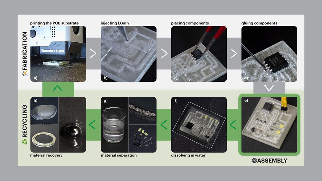
A team of researchers from the University of Maryland, Georgia Tech, and the University of Notre Dame created a new 3D printing method for building PCBs that can use fully recyclable materials. That means a PCB can be created, dissolved, and the materials entirely reused to create a new PCB.
According to the paper (via ResearchGate), this technique, called DissolvPCB, utilizes polyvinyl alcohol (PVA) as a printing filament to form a substrate with hollow channels, where eutectic gallium-indium (EGaIn) liquid metal is injected.
The printed circuit board (PCB) can then be immersed in water, where the PVA completely dissolves. It makes it easy to separate the components, allowing the team to reclaim the liquid metal and extract the PVA from the solution for extrusion. This will enable the team to reuse the materials, with recovery rates of up to 99.4% for the PVA and 98.6% for the EGaIn.
This technique is particularly for experimentation and prototyping, as you don’t have to order or print multiple PCBs for every iteration. It’s also much more sustainable than FR-4 PCBs, which are far more difficult to recycle. These often require a complex, multi-stage process that involves manual dismantling, shredding, and crushing, as well as the use of hazardous chemicals and high temperatures for treatment.
The team also developed a FreeCAD plugin that enables the conversion of KiCad PCB designs into a compatible format for FDM 3D printing. This means you don’t have to manually convert your PCB design to make it compatible with the PVA and liquid metal used in this technique. It also supports through-hole and surface-mounted components, ensuring you can use DissolvPCB on a variety of circuit designs.
Furthermore, the team suggests that the method can be applied to 3D circuit topologies and shape-changing devices. DissolvPCB has been tested to support currents of up to 5A, which makes it compatible with USB-IF’s maximum supported current. It also works with high-frequency signals up to 10 MHz, allowing you to use it for synchronizing and testing devices reliably.
You would likely not use this PCB building technique in durable electronics, such as phones or computers. However, they’re great for engineering labs and makerspaces that frequently experiment with different circuits. Aside from reducing e-waste, it will also likely help engineers and researchers save money, as they no longer have to order new materials for every prototype they build.
Follow Tom's Hardware on Google News to get our up-to-date news, analysis, and reviews in your feeds. Make sure to click the Follow button.