If there's one tech product where scaling doesn't work quite as well, it's DRAM. There are a number of reasons for this, the most important being the actual design of DRAM cells and how it relates to fabrication. But according to Lam Research, the end result of these scaling difficulties means that researchers in the DRAM field may be out of ways to increase DRAM's density scaling as early as five years from now.
It's in this context that Lam Research, a company specializing in semiconductor circuit design, has published a proposal for how future DRAM products may evolve. And that future may very well be 3D, so it seems that memory cubes aren't that far outside the realm of possibilities. According to the company, it'll take us around five to eight years to be able to design a manufacturable 3D DRAM device, leaving the world with a possible three-year gap between the moment 2D DRAM scaling ends and 3D DRAM scaling picks up.
Using their proprietary SEMulator3D software, Lam Research iterated on possible 3D DRAM designs. Their focus was on solving scaling and layer stacking challenges, capacitor and transistor shrinking, inter-cell connectivity, and via arrays (such as TSMC's TSV [Through Silicon Vias], which we've seen in other 3D semiconductor designs already). Finally, the company laid down the process requirements that enable fabrication of their proposed design.
Due to the way DRAM cells are designed, it won't be possible to simply lay 2D DRAM components on their side in order to then stack them on top of each other. This happens because DRAM cells have a high aspect ratio (they're taller than they are thick). Laying them on their side would need lateral etching (and filling) capabilities that are beyond our current capacity.
But when you understand the architecture itself, you can change it and adapt it while attempting to flow around design constraints. This is easier said than done, however, and there's a reason we don't already have 3D DRAM.
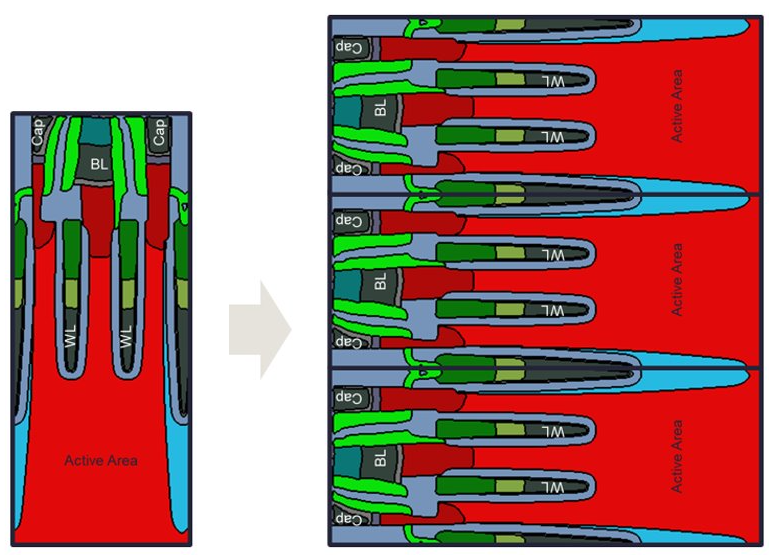
Current DRAM circuit designs need essentially three components: a bitline (a conductive structure that injects current); a transistor that receives the bitline's current output and serves as the gate controlling whether electrical current can flow into (and fill) the circuit; and a capacitor, where the current that flows through the bitline and transistor is ultimately stored in the form of a bit (0 or 1).
Lam Research used a few chip design "tricks" to reach a working architecture. For one, they moved the bitline over to the opposite side of the transistor; because the bitline is no longer surrounded by the capacitor, this means that more transistors can be connected to the bitline itself, improving chip density.
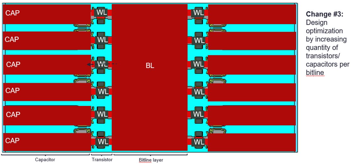
In order to maximize area density gains, Lam Research also applied a few state-of-the-art transistor manufacturing techniques. These include Gate-All-Around (GAA) forksheet designs, which Intel seems to be exploring for next-generation gating technologies. The redesigned DRAM architecture proposed by Lam research can then be stacked, with layers upon layers of the new DRAM cell design on top of one another in a process not unlike that of NAND.
But while NAND scaling is currently around the 232-layer mark, Lam Research estimates that the first generation of a 3D DRAM design such as its own would only leverage up to 28 stacked layers. With the architecture improvements and additional layering, Lam Research estimates that a two-node jump improvement in DRAM density can be achieved — with further improvements being possible through adding additional layers to the DRAM skyscraper. As we've seen in other fabrication technologies, the usage of a via array (the technology underpinning TSMC's TSV) is then used to interconnect individual layers.
There is however an immediate problem with the design proposed by Lam Research: There are no current manufacturing tools that can reliably fabricate the needed features. The company is quick to point out that DRAM design itself lives at the bleeding edge of today; improving and redesigning tools and processes is a common requirement. And as the company puts it, we still have time before we hit the DRAM scaling wall. Hopefully the required tools and expertise will arrive within that time-frame.