Thought AMD's Instinct MI300X and Nvidia's B200 GPUs were huge? Think again: TSMC is working on a version of its chip-on-wafer-on-substrate (CoWoS) packaging technology that will enable system-in-packages (SiPs) over two times bigger, the company announced at its North American Technology Symposium. These will use 120x120mm monstrous packages and will draw kilowatts of power, the foundry envisions.
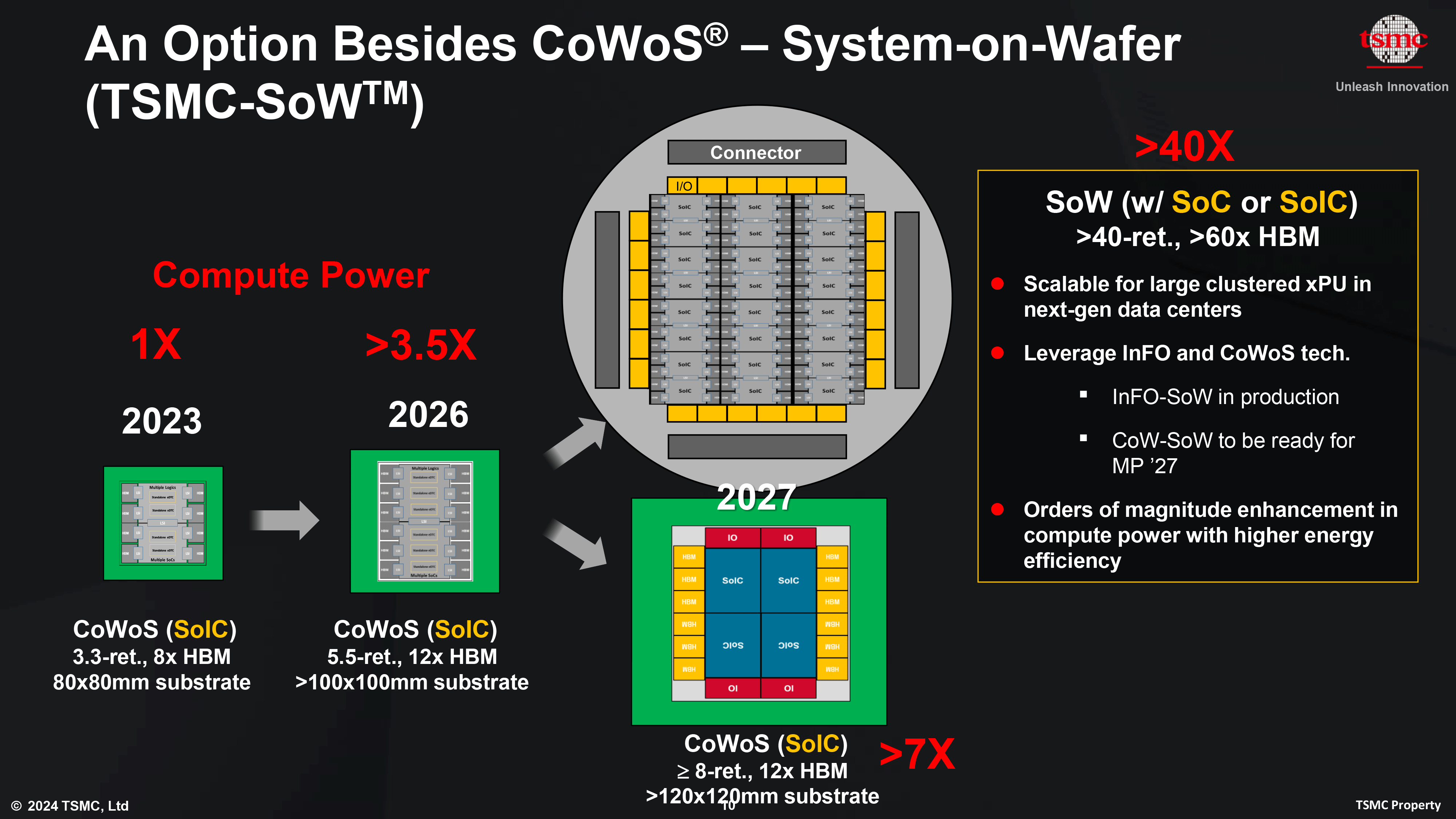
The latest version of CoWoS allows TSMC to build silicon interposers that are about 3.3 times larger than the size of a photomask (or reticle, which is 858mm2). Thus, logic, eight HBM3/HBM3E memory stacks, I/O, and other chiplets can occupy up to 2831 mm2. The maximum substrate size is 80×80 mm. AMD's Instinct MI300X and Nvidia's B200 use this technology, though Nvidia's B200 processor is bigger than AMD's MI300X.
The next generation CoWoS_L, due to be ready for production in 2026, will be capable of enabling interposers of around 5.5 times the reticle size (which may not be as impressive as the 6x reticle size announced last year). This means 4719 mm2 will be available for logic, up to 12 HBM memory stacks, and other chiplets. Such SiPs will also require larger substrates, and based on TSMC's slide, we are looking at 100x100 mm. As a result, such processors will not be able to use OAM modules.
TSMC won't stop there: In 2027, it will have a version of CoWoS technology that will enable interposers eight or more times the reticle size, which will give chiplets 6,864 square mm of space. One of the designs that TSMC envisions relies on four stacked systems-on-integrated chips (SoICs) mated with 12 HBM4 memory stacks and additional I/O dies. Such a giant will certainly draw an enormous amount of power — we are talking about thousands of watts here and will need a very sophisticated cooling technology. TSMC also expects such solutions to use a 120x120mm substrate.
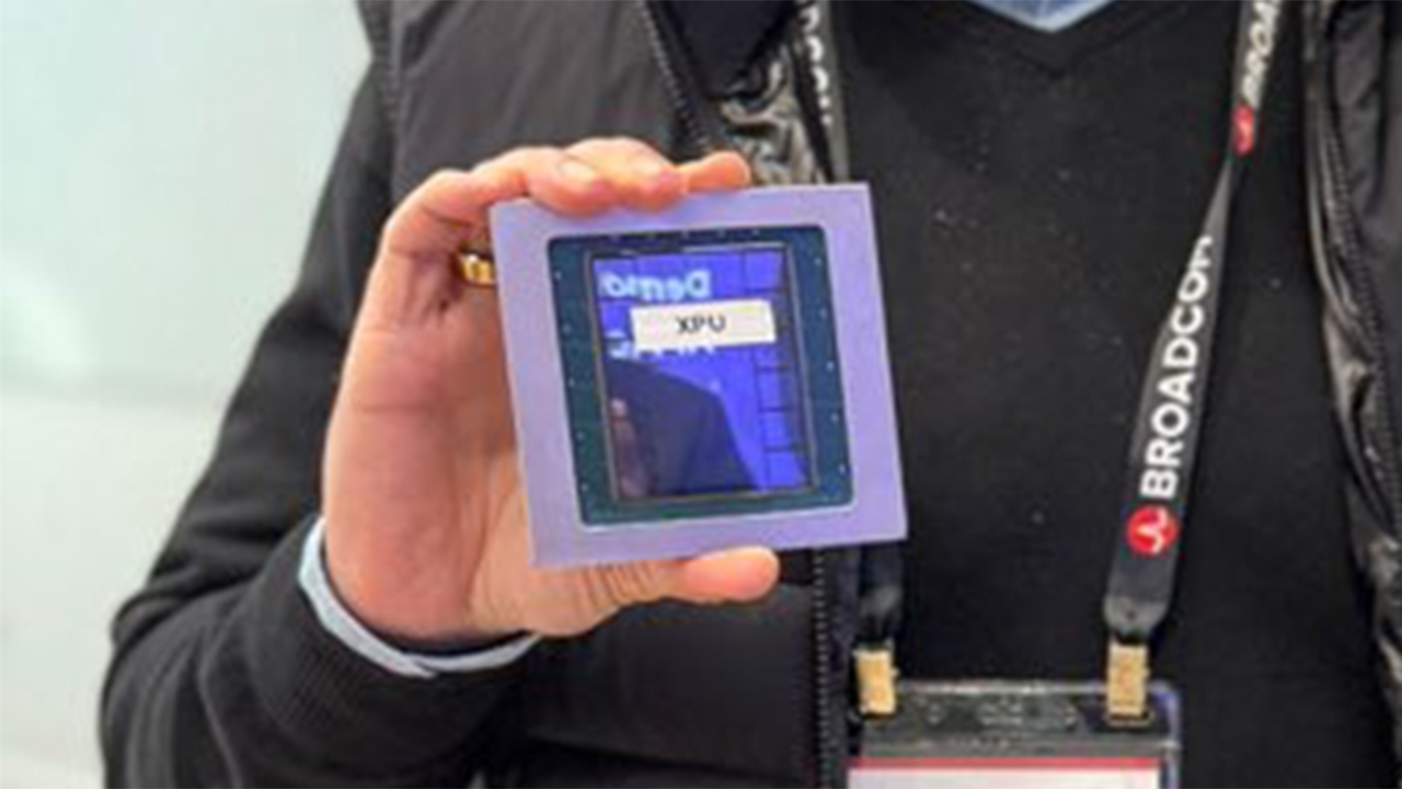
Interestingly, earlier this year, Broadcom demonstrated a custom-built AI processor featuring two logic dies and 12 HBM memory stacks. We do not have specifications for this one, but it looks bigger than AMD's Instinct MI300X and Nvidia's B200, though not as big as what TSMC plans for 2027.


.png?w=600)